
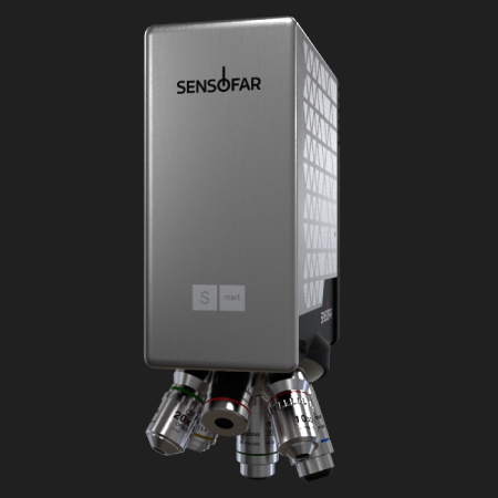

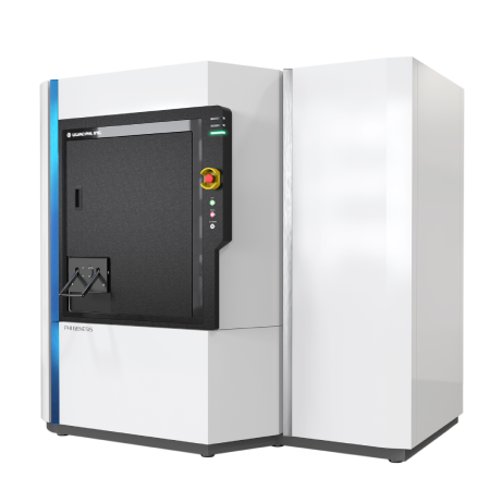
Description
The PHI Genesis is the latest generation of PHI’s highly successful multi-technique XPS product line with PHI’s patented, monochromatic, micro-focused, scanning X-ray source. It is an easy to use, fully automated system with auto-tuning and calibration and multiple parking positions for high throughput. The fully integrated multi-technique platform of the PHI Genesis offers an array of optional excitation sources, sputter ion sources, and sample treatment and transfer capabilities. These features are essential in studying today’s advanced materials and in supporting your material characterization and problem-solving needs.
PHI Genesis offers high sensitivity and high throughput for large area and small area down to 5 µm and unique high-throughput non-destructive depth profiling using optional hard X-ray Cr source. The instrument is fully customizable to address all analytical needs.
PHI Genesis’ Features and Benefits:
Intuitive Sample Navigation And Confident Analysis Area Identification
- The unique scanning X-ray microprobe allows SEM like navigation with point-and-click control
- X-ray induced secondary electron imaging (SXI) provides a perfect correlation between imaged areas and spectroscopy
- SmartMosaic for large-area SXI navigation and large area chemical mapping.
The Only Fully Automated High-Throughput Lab-Based Multitechnique XPS/HAXPES Instrument on the Market Commercially Available
- Large sample handling
- Multiple parking positions
- Automated sample transfer and handling
- Fast automated switching between XPS and HAXPES modes
Optimized Depth Profiling
- Multiple ion gun options (monatomic Ar, C60, argon cluster GCIB) for a variety of organic, inorganic, and mixed materials
- 4-axis stage functionality including rotation/tilt and heating/cooling during sputtering
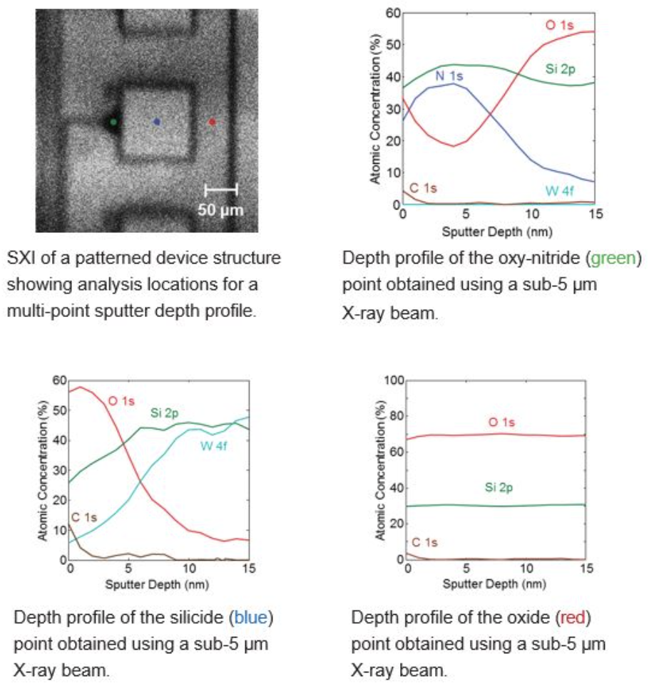
- Multipoint profiling within a single sputter crater for on/off defect analysis and precious samples
- Adjustable solid collection angle for improved angular resolution for Angle-Resolved analysis with advanced software for high-throughput film structure analysis
Superior Micro-Area Analysis
- Highest small area sensitivity on the market
- <5 microns microprobe size in x and y for Al X-ray source and <14 microns for Cr X-ray source
- Image registration for unattended automated micro-area analysis
Bring HAXPES synchrotron capabilities into your lab with the PHI Genesis
- Analytical information depth using the Cr X-ray source is about 3 times deeper than with Al x-ray source
- Probing thicker film structures and buried interfaces, minimizing the effects of surface contamination and ion-induced chemical damage during depth profiling
Suite Of Specialized Solutions For In Situ Characterization Of Advanced Materials
- Electronic band structure of organic and inorganic materials using UPS, LEIPS, REELS measurement from the same sample location
- Electrochemical (biasing, polarization studies) experiments
- Inert sample transfer vessel
- Fully integrated high energy and high spatial resolution Auger Spectroscopy with elemental mapping at the exact location of interest as XPS
Exceptional Capabilities of the PHI Genesis
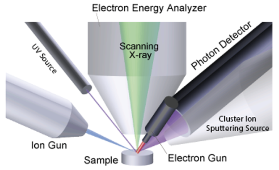
Micro-Focused Scanning X-ray Source and SEM-Like Operation:
| Ease of navigation and operation in SEM-like mode |
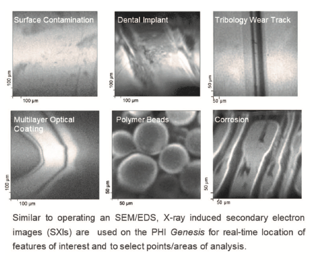
SEM-LIKE XPS MICROPROBE Unique Capabilities: PHI’s scanning XPS microprobe instrument platform provides scanning X-ray induced secondary electron images (SXI) generated by scanning a focused sub-5 μm X-ray beam across the sample. Just like an SEM, SXI’s can be used to navigate to areas of interest and to select areas for analysis in real time. SXI images provide 100% confidence in locating small features of interest and in avoiding areas with contamination and inhomogeneities for analysis. Smart Mosaic allows a user to set up a mosaic acquisition of SXI images from large areas. Stitched mosaic SXI images can be used to investigate the homogeneity of the sample across much larger areas
|
|
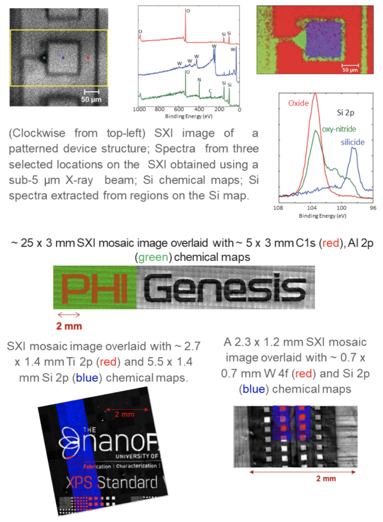
HIGH-SENSITIVITY SPECTRAL AND IMAGING ANALYSIS A typical XPS analysis on the PHI Genesis begins by collecting an SXI image that is quickly generated using a sub-5 μm diameter raster scanned X-ray beam. Areas of interest for small or large spectral analysis or imaging are selected and used to guide the next steps which may include: obtaining high energy resolution spectra for chemical state analysis, chemical state images, or compositional sputter depth profiles. Multispectral chemical maps can be acquired from areas of any size and stitched into a single large area chemical map. Overlays with a variety of color maps and transparency display options can be used to highlight areas that are spatially and chemically distinct.
|
|
|
|
Optimized Thin Film Depth Profile Analysis:
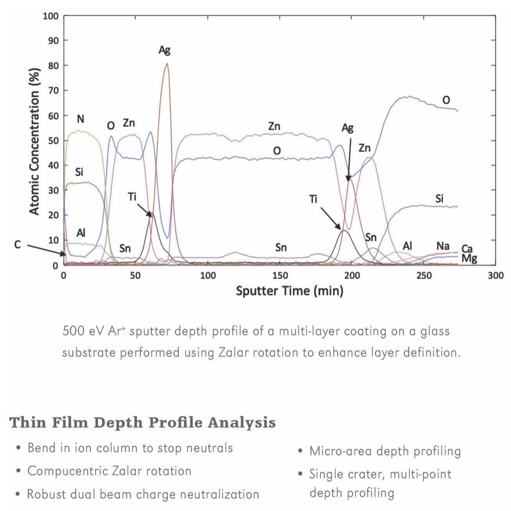
OPTIMIZED CONFIGURATION A focused X-ray beam, high sensitivity spectrometer, high performance floating column argon ion gun, automated dual beam charge neutralization, Zalar rotation, and advanced data reduction algorithms provides the highest performance XPS depth profiling capability available. The standard monatomic argon ion gun can generate 5 eV to 5 keV Ar+ ion beams and is ideally suited for most inorganic depth profiling applications. |
|
 ARGON GAS CLUSTER ION BEAM (GCIB) OPTION FOR ORGANIC DEPTH PROFILING ARGON GAS CLUSTER ION BEAM (GCIB) OPTION FOR ORGANIC DEPTH PROFILING
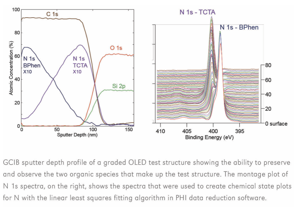
It is well known that monatomic Ar ion guns commonly used for inorganic thin film analysis typically cause severe chemical damage when sputtering most polymer and organic materials. PHI has led the way in developing and applying cluster source ion guns for the successful thin film analysis of polymer and organic materials. Our optional 20 kV Argon gas cluster ion beam (GCIB) and optional C60 ion gun have proven performance for depth profiling many polymer and organic films while minimizing the potential for chemical damage.
|
|
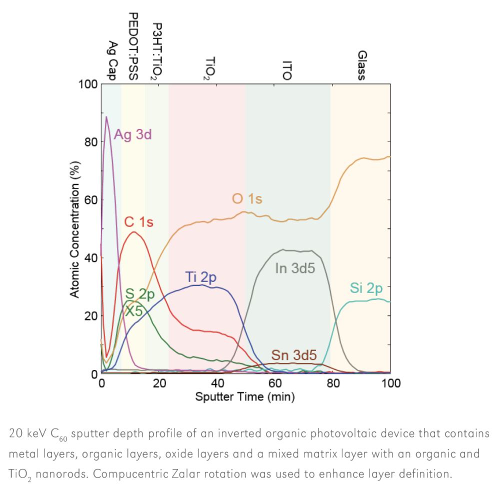
C60 CLUSTER SOURCE ION GUN OPTION FOR MIXED MATRIX DEPTH PROFILING With the introduction of cluster source ion guns for organic and polymer thin film depth profiling, interest has grown in applying these ion guns to inorganic structures that sustain chemical damage with monatomic Ar ion beam sputtering. Our experience has shown that some metalloids, oxides, and thin film structures that contain both organic and inorganic materials sustain less chemical damage and differential sputtering artifacts when depth profiled using a 20 kV C60 cluster source ion gun. |
Complete Electronic Band Structure Characterization:
MEASUREMENT AT THE SAME LOCATION FOR XPS, UPS, LEIPS AND REELS In the PHI Genesis, LEIPS, UPS, Argon and GCIB ion beams, and neutralization beams are all aligned to the XPS measurement position. This allows for comprehensive evaluation of organic semiconductor materials. |
|
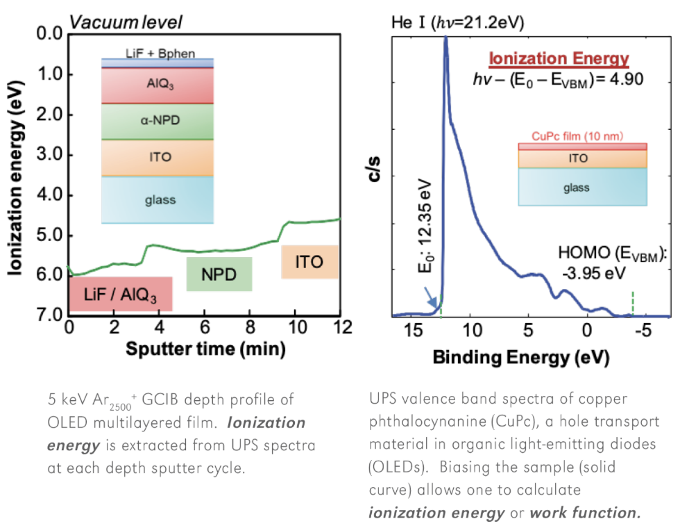
ULTRAVIOLET PHOTOELECTRON SPECTROSCOPY (UPS) – VALENCE BAND Design of complex electronic material systems for display panels, flexible circuitry, and photovoltaics require knowledge of the basic properties of each component’s band structure in order to achieve efficient charge transport. The combination of ultraviolet photoelectron spectroscopy (UPS) and low energy inverse photoemission spectroscopy (LEIPS) provides a complete characterization of the valence and conduction bands, as well as useful parameters such as the band gap, ionization energy, work function, and electron affinity. Samples provided by: Organic Optoelectronics Practical Development Center(i3-opera) |
|
COMBINED MEASUREMENTS FROM UPS AND LEIPS LEIPS provides accurate values of electron affinity (EA) which is required for designing organic light-emitting diode, understanding band structure at metal-semiconductor and heterojunctions and in studies of charge-transfer processes.semiconductor. Low energy incident electrons (<5 eV) used in this technique are well-suited for analysis of organic materials with minimal damage. The ionization energy can be obtained from the highest occupied molecular orbital (HOMO) of the UPS measurement. The electron affinity can be obtained from the lowest unoccupied molecular orbital (LUMO) of the LEIPS measurement. From the difference in those two values, the semiconductor bandgap energy can be calculated. |
|
COMBINED MEASUREMENTS FROM UPS AND LEIPS
|
|
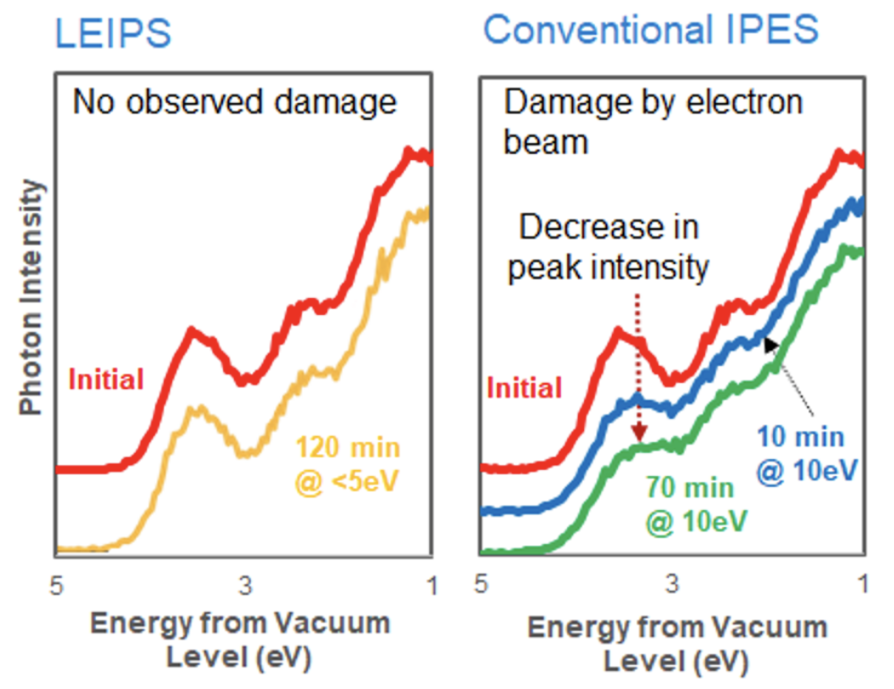
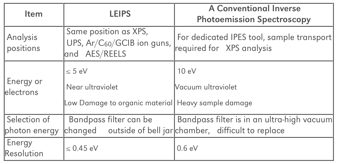
LOW DAMAGE ANALYSIS OF ORGANIC MATTER A comparison of the degree of electron beam damage on a thin film C60 sample using LEIPS electron energies and conventional IPES energies is shown. When the sample was irradiated with 10 eV electrons, equivalent to conventional IPES, the spectral shape changed, indicating that electronic damage had occurred. On the other hand, in the LEIPS measurement using 5 eV of electron energy, there is no change in the spectrum after extensive measurement time, suggesting that no sample damage has occurred. |