Discount Products: Look through products available for a 25% – 50% discount in 2020. The items provided on a first come, first serve basis. View Discounted Products
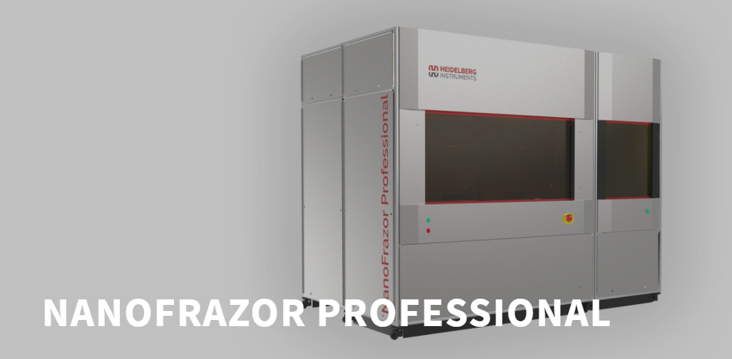
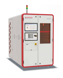
Introducing the Heidelberg Instruments NanoFrazor Professional
The NanoFrazor Professional is a platform that can be customized to meet individual requirements for industrial and prototyping applications. It combines all the unique NanoFrazor capabilities with a specially designed 8-inch wafer platform and an adapted high-speed piezo scanner for moving the tip. Various extensions can be added to increase speed, placement accuracy or automation. The NanoFrazor Professional is designed for process development of next generation semiconductor nodes, mastering for nanoimprint lithography, and manufacturing devices with nano-features in small areas.
With the direct laser sublimation module, nano- and microstructures can be seamlessly and quickly written into the same resist layer in a single fabrication step.
Key Features
High-resolution
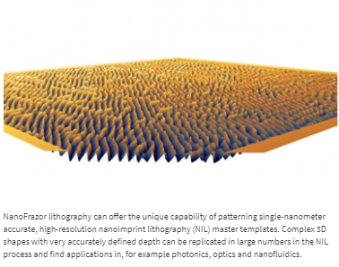
Easy patterning of nanostructures even with complex geometries; min. lateral features 15 nm; vertical resolution 2 nm
Thermal Scanning Probe Lithography
New approach to nanopatterning enabling applications not otherwise feasible
Non-invasive Lithography
No damage from charged particles, no proximity effects, clean lift-off
Compatibility
With all standard pattern transfer methods: lift-off, etching, nanoimprint lithography, etc – knowledge resource and best practices available in our “Recipe Book”
In-situ Imaging
Immediate control of patterned structures
Precise Overlay and Stitching
Markerless overlay and stitching accuracy 25 nm specified, sub-10 nm overlay shown
Unique Thermal Cantilevers
Integrated microheater and distance sensor; easy to exchange and economical
IDecapede Module
10-tip write head for 10-fold increase in throughput for high-resolution patterning
Laser Sublimation Module
High-throughput exposure of coarse structures in the same exposure step; 405 nm wavelength CW fiber laser
Vibration Isolation
Three-layer acoustic and superior vibration isolation (> 98% @ 10 Hz)
Low Cost of Ownership
No need for cleanroom, vacuum pump or expensive consumables
Key Benefits
In-situ imaging enables two unique features: markerless overlay, and comparison of the written and target patterns during writing so that the parameters can be immediately adjusted. This approach, called closed-loop lithography, results in sub-2 nm vertical precision for 2.5D (grayscale) shapes of any complexity. Fast and precise control of a heated nanoscale tip enables innovation not otherwise feasible.
Laser Sublimation Module
High-throughput exposure of coarse structures in the same exposure step
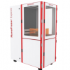
Glovebox Integration
Customized solution in collaboration with MBraun with minimized vibrations for work in controlled atmosphere
Trust the Experts at Spectra Research Corporation
Spectra Research Corporation (SRC) offers a range of innovative high-quality scientific products and laboratory services to industrial and scientific markets throughout Canada.