Discount Products: Look through products available for a 25% – 50% discount in 2020. The items provided on a first come, first serve basis. View Discounted Products
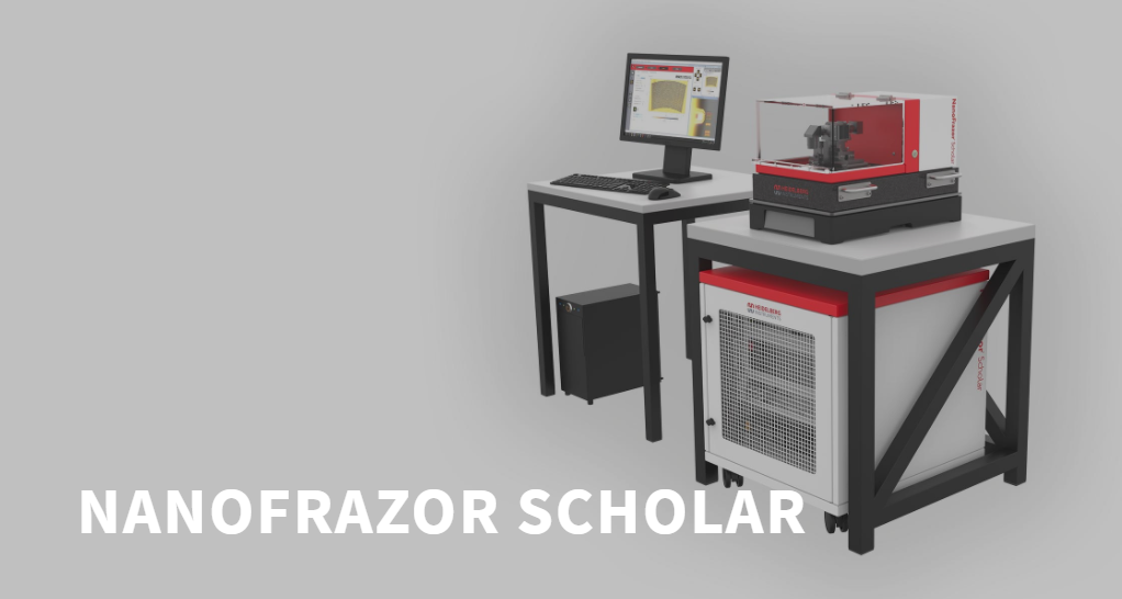
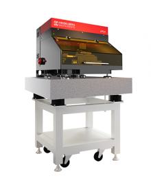
Introducing the Heidelberg Instruments NanoFrazor Scholar
Heidelberg NanoFrazor Scholar is particularly suitable for academic research groups requiring an affordable system for nanofabrication. NanoFrazor Scholar is used for nanopatterning of quantum devices on 1D/2D materials such as quantum dots, Dolan bridges and Josephson junctions, and nanoscale arrays. Its unique capabilities enable new devices in new materials. For example, it is used for advanced applications such as grayscale photonics devices, nanofluidics structures or biomimetic substrates for cell growth; local modification of materials by heat, e.g. chemical reactions and physical phase changes.
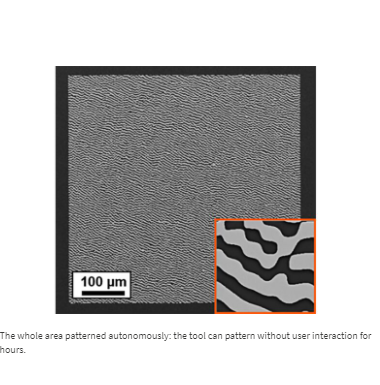
In-situ imaging enables two unique features: markerless overlay, and comparison of the written and target patterns during writing so the parameters can be immediately adjusted. This approach, called closed-loop lithography, results in sub-2 nm vertical precision for 2.5D (grayscale) shapes of any complexity. Fast and precise control of a heated nanoscale tip enables innovation not otherwise feasible.
Key Features
NANOSCALE MATERIAL CONVERSION.
The heated tip can alternatively be used to induce highly localized modification of materials: Deprotection of functional groups, precursor conversion, amorphization, crystallization, change of magnetic orientation, etc.
OTHER UNIQUE CAPABILITIES
3D grayscale lithography with unprecedented accuracy enabled by closed-loop lithography
Accurate overlay and stitching without artificial markers, achieved by in-situ AFM
Key Benefits
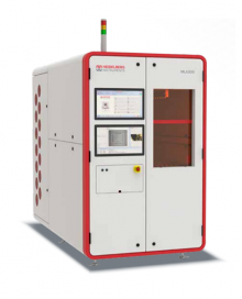
The technology behind the system is the result of more than 20 years of intensive research and development (R&D) that started at IBM Research Zürich and now takes place at Heidelberg Instruments Nano. The NanoFrazor hardware and software are constantly advancing to extend the capabilities and performance of the tool and its range of applications. Our dedicated team of experts continues to develop and optimize the pattern transfer processes for different applications. We compile this know-how in a growing library of best practices and protocols to support our customers.
Trust the Experts at Spectra Research Corporation
Spectra Research Corporation (SRC) offers a range of innovative high-quality scientific products and laboratory services to industrial and scientific markets throughout Canada.
Specifications
Writing performance
Minimum structure size [nm]
20
Minimum lines and spaces [half pitch, nm]
30
Grayscale / 3D-resolution (step size in PPA) [nm]
3
Writing field size [X μm x Y μm]
50 x 50
Field stitching accuracy (markerless, using in-situ AFM imaging) [nm]
50
Overlay accuracy (markerless, using in-situ AFM imaging) [nm]
50
Write speed (typical scan speed) [mm/s]
0.5
Write speed (50 nm pixel) [μm²/min]
500
AFM imaging performance
Lateral imaging resolution (feature size) [nm]
10
Vertical resolution (topography sensitivity) [nm]
0.2
Imaging speed (@ 50 nm resolution) [μm²/min]
500
System features
Substrate sizes
1 x 1 mm² to 50 x 50 mm², 0 – 20 mm thickness (100 x 100 mm² possible with limitations)
Optical microscope
3.6 μm optical resolution, 1.5 mm x 1.1 mm field of view
Magnetic cantilever holder
Fast (< 1 min) and accurate tip exchange
Housing
Compact housing with separate controller rack, active vibration isolation (small footprint) or passive vibration isolation (slightly better performance) included.
Software features
GDS and bitmap import, AFM image analysis and drawing for overlay, fully automated calibration routines, Python scripting
NanoFrazor cantilever features
Integrated components
Tip heater, topography sensor, electrostatic actuation
Tip geometry
Conical tip with < 10 nm radius and 750 nm length
Tip heater temperature range
e 25 °C – 1100 °C (< 1 K setpoint resolution)
System dimensions & installation requirements
Height × width × depth
50 cm x 32 cm x 30 cm
Weight
100 kg
Power input
1 x 110 or 220 V AC, 10 A
Gas input
Compressed air (> 4 bar) for passive vibration isolation
Vibration and noise level
Ambient acoustic noise levels need to be kept below 40 dB for best performance. A strong table is required if the active vibration isolation is chosen. Floor requires vibration level VC-B.
Other considerations
Recipe book with detailed descriptions of various processes is included (regularly updated with software).
Cantilever tips degrade over time (> 50 h patterning possible). Exchange is fast and low cost for tool owners.
A cleanroom or special laboratory is not required. No vacuum needed.
Unique capabilities make it easy to receive government funding (for system itself or later research projects)