Discount Products: Look through products available for a 25% – 50% discount in 2020. The items provided on a first come, first serve basis. View Discounted Products
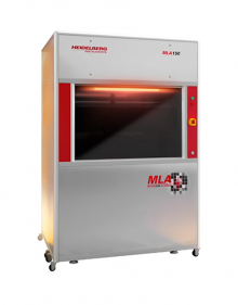
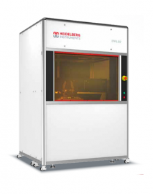
Introducing the Heidelberg Instruments μMLA THE TABLE-TOP MASKLESS ALIGNER
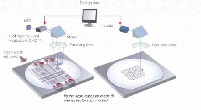
The Maskless Aligner was first introduced in 2015. Since then, the revolutionary, state-of-the-art maskless technology has become firmly established. The μMLA presents a new generation of tabletop laser lithography tool: Configure the set-up precisely to your needs with raster scan and vector scan mode (or both) and a variable resolution write head.
In many applications, the traditional photomask has become a thing of the past as your design file is exposed directly onto the resist-coated wafer via a 2-dimensional Spatial Light
Modulator (SLM). The µMLA is the direct successor of the MLA100 and is the „little brother“ of our Advanced Maskless Aligner MLA150, which serves as a trusted, indispensable workhorse in
many multi-user facilities, nanofabrication labs, and national institutes.
In the development of our brand-new entry-level system µMLA, we introduced new features such as variable resolution and created a table-top system that is flexible and highly customizable. And of course small sample handling is straightforward. Building on our many years of experience, the µMLA features all that was best in our previous tabletop systems, while offering more options and higher performance than ever before. Raster scan exposure mode (l) and/or vector scan more (r)
Applications include Research & Developent in areas such as MEMS, micro-fluidics, micro-optics and all other fields ere an affordable, compact, and powerful pattern generator for microstructures is required.
Key Features
Two Exposure Modes
The µMLA allows you to either choose between Raster Scan Exposure Mode and Vector Mode, or to even run both exposure modes on one and the same system! The Raster Scan Exposure mode is fast and provides excellent image quality and fidelity, while the write time is independent of structure size or pattern density. The Vector Scan Mode can be helpful for exposing designs consisting of curved lines,
where smooth contours are required. While Vector Mode creates similar image quality as the Raster Scan exposure mode, it cannot achieve the same write speed, especially for patterns with high fill factor.
A Choice of Wavelengths
In consequence, you can use up to three differentwavelengths (LED and/or laser diodes) on one system.
Variable Resolution
Our newly developed variable resolution function allows you to choose up to three different resolutions for a particular write mode. Simply select the resolution of choice in the software menu and optimize the parameters for your application.
The Surface at One Glance
The optional overview camera provides an easy way to locate alignment marks or other features of interest on your substrate.
Small Sample Handling
Small sample handling is straightforward with the μMLA: The optical autofocus option allows accurate exposure right up to the edges of a sample
Key Benefits
GRAYSCALE LITHOGRAPHY
The μMLA also offers a standard Grayscale mode, which allows the creation of structures for a wide range of applications in micro-optics. This example shows micro-lenses written in 15 μm thick AZ4562, with a pitch of 30 μm and a radius of curvature of 16 μm.
COMPLEX PATTERNS
Binary diffractive optical element comprised of 1µm² squares and exposed into 500 nm thick Shipley S1805.
MICROFLUIDICS
A microfluidic system patterned using uMLA.
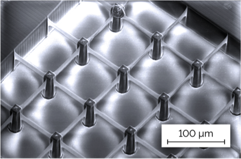
UNIVERSAL PATTERNING OF MICROSTRUCTURES
Concentric rings with 1-μm line width were written into the photoresist using the Raster Scan exposure mode.
PRECISE ALIGNMENT
Single Ni nanowires (horizontal line in the image) with two precisely aligned thermometer structures used to investigate Co-Ni alloy magneto-thermopower and magneto-resistance.
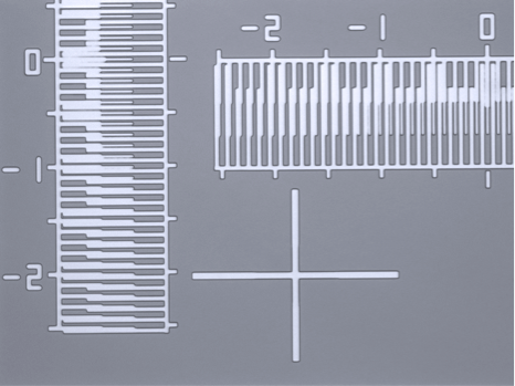
PRECISE ALIGNMENT
In many applications, several layers need to be exposed on the same substrate. The μMLA’s cameras can automatically detect alignment markers and adjust the position, rotation, scaling and orthogonality of the exposure to the existing structures. The image shows Vernier scales and a “cross-in-cross” structure, employed to measure the remaining offset in x and y direction.
Trust the Experts at Spectra Research Corporation
Spectra Research Corporation (SRC) offers a range of innovative high-quality scientific products and laboratory services to industrial and scientific markets throughout Canada.
Specifications
Writing performance (both Raster Scan and Vector Exposure Module)
Write Mode I
Write Mode II
Minimum structure size [μm]
0.6
1
Minimum lines and spaces [half pitch, μm]
0.8
1.5
2nd layer alignment over 5 x 5 mm2 [3σσ, nm]
500
500
2nd layer alignment over 50 x 50 mm2 [3σσ, nm]
1000
1000
Writing performance with the Raster Scan Exposure Module
Line width variation [3σσ, nm]
200
300
Max. write speed [mm2/min]
10
30
Write speed with optional “Variable Resolution for
Raster Scan Exposure Module” (UMVAR)
for different minimum structure sizes
10 mm²/min at 0.6 µm
20 mm²/min at 1 µm
25 mm²/min at 2 µm
30 mm²/min at 1 µm
60 mm²/min at 2 µm
100 mm²/min at 4 µm
Writing performance with the Vector Exposure Module