|
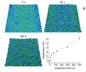
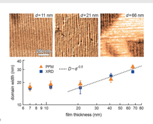
Asylum Research Cypher™ and MFP-3D™ atomic force microscopes (AFMs) provide valuable information for characterizing thin films and coatings. They quantify 3D roughness and texture with unmatched spatial resolution and measure nanoscale functionality including electrical, magnetic, and mechanical behavior. Thin films and coatings play a critical role in everything from food containers to photovoltaics. To meet such varied needs, they are made from every class of material and by numerous processes including physical and chemical vapor deposition techniques, atomic layer deposition, and sol gel processing.1 A key step in developing any new film is characterizing its surface structure and physical properties, whether in engineering commercial products (Figure 1) or pursuing fundamental materials science (Figure 2). The intrinsic dimensions of films (thickness, grain and domain sizes, etc.) make it important to characterize them on sub-nanometer to micrometer length scales. The AFM is a powerful tool for this purpose for many reasons. For instance, it possesses much higher spatial resolution than other stylus or optical-based methods.4 Samples need not be optically reflective or electrically conducting, allowing access to virtually any film. AFMs also provide complementary information to electron microscopes, such as accurate 3D surface profiles, and offer a more flexible operating environment for work at both ambient and non-ambient atmospheres and temperatures. Here we describe the extensive features of Asylum Research AFMs for thin film characterization and show examples over a range of applications. With today’s AFMs, surface roughness can be measured more accurately, quickly, and easily than ever before. A wider array of built-in analysis tools and automated routines mean higher productivity and greater ease of use. Also, research and instrumentation advances have created a variety of AFM modes for measuring nanoscale film functionality including electrical, magnetic, and mechanical response.
|
|