

Description
|
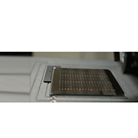
Our standard lithography systems can accommodate substrates of arbitrary shapes with lateral dimensions of up to 1400 x 1400 mm2. Larger substrates require specially designed systems, in which the substrate is stationary and the exposure unit is moved during the writing process. We have designed and installed these types of systems for fabrication of linear encoders with dimensions of 3100 x 50 mm2 and for large area photomask production with an area up to 2400 x 1900 mm2 – the latter system is also equipped with a fully automatic handling system. Besides lateral dimensions, substrates also differ in thickness and material properties. Our standard systems can handle all common semiconductor materials. We have developed special chuck and loader designs for very thin flexible substrates for sizes up to 1400 x 1400 mm2. Some applications require exposures on existing structures with varying height, e.g. in deep etched groves. Heidelberg Instruments offers a special writing strategy for such applications.
|
 |
|
 |
||
 |
||
Freeform Systems
- Applications for implementation of electronic systems
- Non-planar surfaces
- Imaging sensors
- Artificial vision
- Integrated micro-optics
Tabletop Micro Pattern Generator
Key Features and Options
| Substrates up to 6“ x 6“ |
| Structures down to 0.6 μm |
| Address grid down to 20 nm |
| Basic gray scale exposure mode |
| Real time auto focus system |
| Standard or UV diode laser source |
| Vector and raster exposure mode |
| Exchangeable write modes |
| Camera system for alignment |
| Multiple data input formats |
Deep UV Lithography Systems
The laser sources in our standard systems range from 355 nm to 532 nm, making it possible to expose all the standard UV photo resists. However, for special applications resists sensitive at even shorter wavelengths are required. At the same time it is possible to create even smaller features because of the smaller wavelength. That […]