
RC and Heidelberg Instruments are conducting a seminar tour to show the remarkable capabilities of NanoFrazor nanolithography 2D and 3D systems.
 |
 |
||
 |
 |
 |
 * Click on the applicable city name above to register
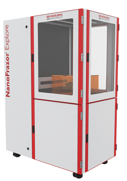
Based on thermal scanning probe lithography developed at IBM Research, NanoFrazor lithography is the fastest and most versatile of all scanning probe lithography techniques.This new lithography system’s applications include:
- High-quality metal contacting of 2D materials
- Tuning photonic molecules
- Generating nanofluidic devices
- Generating spintronic circuits
Register for one of the upcoming seminars to see NanoFrazor lithography in action!
* For more information on the seminar nearest you, please use the linked city names above.