SRC will represent Orion Additive Manufacturing systems in Canada, helping research and industrial teams produce stronger, denser, end-use polymer parts using Thermal Radiation Heating technology.
MISSISSAUGA, Ontario — June 28, 2026 — Spectra Research Corporation, a Canadian supplier of advanced scientific instruments and research technologies, is pleased to announce its partnership with Orion Additive Manufacturing GmbH, a developer of industrial 3D printing systems for high-performance polymers.
Through this partnership, SRC will represent Orion AM technologies in Canada, supporting universities, government laboratories, industrial R&D facilities, medical research groups, aerospace manufacturers, and advanced manufacturing organizations seeking stronger, denser, and more reliable polymer additive manufacturing solutions.
Orion AM specializes in industrial 3D printing systems for advanced engineering polymers including PEEK, PEI/ULTEM, PPSU, PAEK, PEKK, PC, and other high-performance thermoplastics. These materials are widely used in demanding environments where mechanical strength, thermal resistance, chemical stability, and dimensional reliability are critical.
A central innovation behind Orion’s platform is Thermal Radiation Heating, a proprietary high-temperature additive manufacturing process designed to heat the printed material itself rather than relying only on heated chamber air. This approach helps improve layer fusion and addresses common limitations in conventional FFF and FDM polymer 3D printing, including warping, distortion, delamination, weak interlayer bonding, porosity, and anisotropic mechanical performance.
“Many Canadian researchers and manufacturers are interested in high-performance polymer 3D printing, but conventional systems often struggle to deliver the mechanical reliability required for end-use parts,” said Serge Dandache, General Manager – Spectra Research Corporation. “Orion’s Thermal Radiation Heating technology directly addresses one of the most important challenges in polymer additive manufacturing: achieving strong, fully bonded structures from advanced materials such as PEEK, PEI, and PPSU.”
Addressing a Critical Challenge in High-Performance Polymer Additive Manufacturing
High-performance polymers such as PEEK and PEI are attractive for aerospace, medical, industrial, and advanced engineering applications because of their excellent thermal, mechanical, and chemical properties. However, these materials are difficult to print consistently using conventional extrusion-based systems.
In standard FFF printing, the deposited material begins cooling after extrusion. This can create cold joints between print lines and layers, leading to weak bonding, internal voids, reduced part density, and inconsistent mechanical strength. For parts intended for real-world use, these defects can limit the adoption of additive manufacturing for production, qualification, and functional testing.
Orion AM’s Thermal Radiation Heating process is designed to overcome these limitations by allowing thermal energy to penetrate the printed material and promote stronger layer-to-layer fusion. The result is improved internal bonding, denser infill, and more uniform mechanical properties throughout the printed part.
Fully Bonded Structures, Solid Infill, and Unrivalled Strength
Orion’s process has demonstrated important performance improvements for industrial polymer additive manufacturing, including:
Fully bonded structures
Thermal Radiation Heating helps reduce weak interfaces between deposited lines and layers, enabling more homogeneous internal structures.
Solid infill and high density
Orion reports CT scan results showing average void content below 0.05%, corresponding to approximately 99.95% density in printed specimens.
Improved mechanical strength
Orion presents tensile strength data across multiple PEEK materials, demonstrating performance that approaches or, in selected cases, exceeds injection-molded reference values.
Reduced warping, distortion, and delamination
By heating the material directly, Orion’s process helps reduce thermal gradients that often contribute to part deformation and layer separation.
More isotropic performance
Improved interlayer bonding helps reduce the directional weakness commonly associated with conventional FFF polymer printing.
Together, these advantages help move polymer 3D printing beyond prototyping and toward functional end-use components for research, validation, tooling, and production development.
Orion AM Systems Available Through SRC in Canada
SRC will support Canadian customers interested in Orion’s industrial additive manufacturing systems, including:
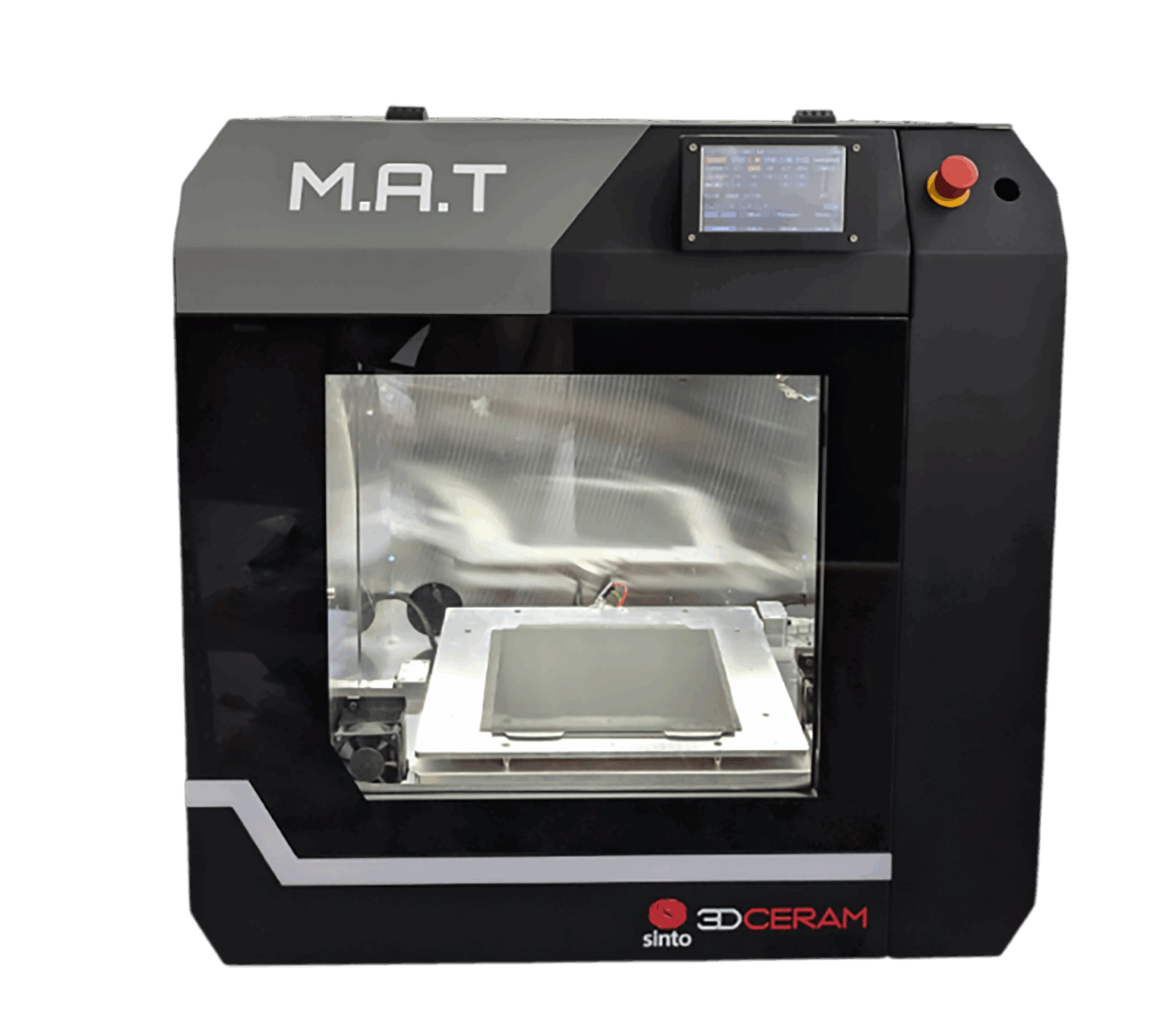
Orion A150 Industrial 3D Printing System
The Orion A150 Series is an industrial additive manufacturing platform designed for high-performance polymer 3D printing with materials such as PEEK, PAEK, PEKK, PEI/ULTEM, PPSU, PC, ABS, PA6, and PA12. The system combines high-temperature polymer processing with Thermal Radiation Heating to improve layer bonding, density, and part strength.
The A150 is suitable for laboratories and industrial teams developing smaller high-performance polymer components, test specimens, application prototypes, and functional end-use parts.
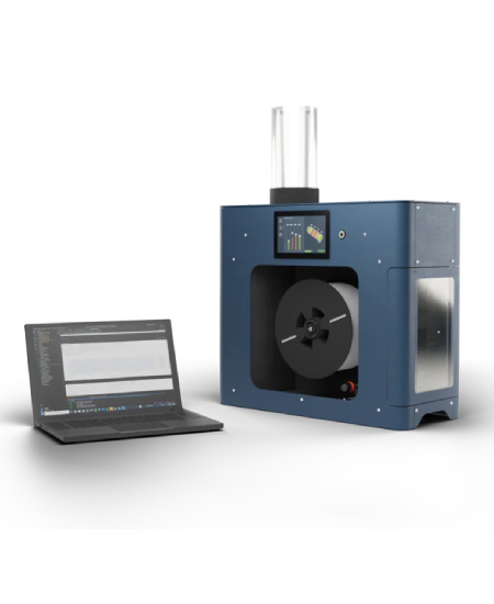
Orion A460 Large-Format Industrial AM System
The Orion A460 extends Orion’s Thermal Radiation Heating platform to larger industrial components. Designed for large-format additive manufacturing with high-performance polymers, the A460 supports materials including PEEK, PAEK, PEKK, PPSU, PEI/ULTEM, PI, PC, and PA.
The A460 is suited for organizations developing larger functional parts, aerospace-grade polymer components, industrial fixtures, tooling, housings, and engineering prototypes requiring high temperature resistance, chemical resistance, and strong mechanical properties.
Supporting Canadian Research and Industrial Innovation
By representing Orion AM in Canada, SRC expands its additive manufacturing portfolio for organizations working in:
- Aerospace and defence polymer component development
- Medical device and implant-related polymer research
- Advanced manufacturing and industrial R&D
- High-temperature polymer materials development
- Functional prototyping and end-use polymer parts
- Vacuum, sealed housing, fluidic, and harsh-environment applications
- University and government laboratory research
- Materials testing, process validation, and polymer AM qualification
“SRC’s role is to help Canadian customers connect the right technology to the right research or manufacturing challenge,” said Serge Dandache. “With Orion, we can support organizations that require more than standard polymer prototyping. This is about enabling strong, dense, high-performance thermoplastic parts for demanding technical applications.”
A Scientific Technology Partner for Canadian Laboratories and Manufacturers
Spectra Research Corporation provides Canadian sales and technical support for advanced scientific and industrial technologies. SRC works closely with global suppliers to help customers evaluate instrumentation, understand technical capabilities, and implement systems effectively in research and production environments.
For Canadian organizations evaluating PEEK 3D printing, ULTEM 3D printing, PPSU additive manufacturing, or industrial high-temperature polymer 3D printers, SRC can help determine whether Orion’s Thermal Radiation Heating technology is suitable for the application, material requirements, part geometry, and production workflow.
Contact SRC to Learn More About Orion AM in Canada
Canadian researchers, engineers, and advanced manufacturing teams interested in Orion AM systems can contact Spectra Research Corporation to discuss system configuration, material compatibility, application requirements, and quotation support.
Contact Spectra Research Corporation
3585 Laird Road, Unit 15 & 16
Mississauga, Ontario, Canada
Phone: 905-890-0555
Toll Free: 1-866-753-4433
Website: Spectra Research Corporation
About Spectra Research Corporation
Spectra Research Corporation is a Canadian distributor and technical partner providing advanced scientific instruments, analytical technologies, and research solutions to universities, government laboratories, industrial R&D facilities, and commercial organizations across Canada. SRC works with leading global suppliers to support research and development in materials science, nanotechnology, spectroscopy, microscopy, surface science, life sciences, additive manufacturing, and advanced industrial analysis.
About Orion Additive Manufacturing
Orion Additive Manufacturing GmbH develops industrial additive manufacturing systems for high-performance polymers including PEEK, PEI/ULTEM, PPSU, PAEK, PEKK, and other engineering thermoplastics. Orion’s Thermal Radiation Heating technology is designed to improve interlayer bonding, reduce warping and delamination, and produce stronger, denser polymer parts for demanding industrial, medical, aerospace, and advanced manufacturing applications.