Broaden your Horizons with the New Sensofar System S wide

New Sensofar System S wide
Learn all about New Sensofar System S wide exceptional 3D Optical Profiler which expands metrology towards a larger field of view for surface roughness measurement. The S wide integrates the benefits of a digital microscope into a hi-resolution, fast scanning measuring instrument.

Key Topics:

  • This new system improve routine operation through ease of use, with one-shot height measurements up to 40 mm, without Z-scanning
  • Achievement of sub-micron height repeatability over entire extended area
  • Color acquisition with the best resolution thanks to the integrated 5Mpx camera
  • Form deviation from 3D CAD models for an effective integration to daily internal processes

Are you visiting us from America?

Wednesday, April 8th, 2020

6:00 PM to 7:00 PM  CEST

Presented by: Daniel Sakakini

Access our webinar from here

Webinar Broaden.png

WEBINARS NANOFRAZOR TECHNOLOGY

NANOFRAZOR INTRODUCTION

Speaker: Dr Felix Holzner, CEO of Heidelberg Instruments Nano

The webinar will be repeated on May 7, 2020, at 08:45 CEST


RESOLUTION AND SPEED

Speaker: Samuel Bisig, Heidelberg Instruments Nano

This webinar will be repeated on May 14, 2020, at 08:45 CEST


CLOSED-LOOP 3D (GRAYSCALE) LITHOGRAPHY

Speaker: Dr Fabian Könemann, Heidelberg Instruments Nano

This webinar will be repeated on May 21, 2020, at 08:45 CEST


MARKERLESS OVERLAY & STITCHING

Speaker: Dr Urs Dürig, Heidelberg Instruments Nano

This webinar will be repeated on May 28, 2020, at 08:45 CEST


INTEGRATED DIRECT LASER SUBLIMATION

Speaker: Dr Simon Bonanni, Heidelberg Instruments Nano

This webinar will be repeated on June 4, 2020, at 08:45 CEST


NANOSCALE HEATING AND NON-INVASIVE PATTERNING

Speaker: Dr Anya Grushina, Heidelberg Instruments Nano

This webinar will be repeated on June 11, 2020, at 08:45 CEST


RESIST MATERIALS & TIP LIFETIME

Speaker: Jonas Vergés, Heidelberg Instruments Nano

This webinar will be repeated on June 18, 2020, at 08:45 CEST


LIFT-OFF PROCESSES

Speaker: Dr Tero Kulmala, Heidelberg Instruments Nano

This webinar will be repeated on June 25, 2020, at 08:45 CEST


HIGH-RESOLUTION ETCHING PROCESSES

Speaker: Dr Emine Cagin, Heidelberg Instruments Nano

This webinar will be repeated on July 2, 2020, at 08:45 CEST


3D PATTERN TRANSFER

Speaker: Dr Tero Kulmala, Heidelberg Instruments Nano

This webinar will be repeated on July 9, 2020, at 08:45 CEST


Note from the Nanoworld‹”Hafnium Oxide Helps Keep Microelectronics on the Moore¹s Law Trajectory”


Getting “Moore” By Using “Haf”

Hafnium oxide helps keep microelectronics on the Moore’s law trajectory

Read the article >

AFM vs. STM: The Resolution Battle

The uneasy truce has been broken, as AFM refuses to concede resolution superiority to STM.

Read the article >

Springtime Beauty at the Nanoscale

Just like the brilliant blooms each spring, STM provides a captivating view of the world in which we live.

Read the article >

Note_Asyleum_3.JPG

What’s Cypher’s High Resolution Secret?

You’ve seen Cypher’s high-resolution results, but what makes it possible? Roger Proksch shares the key secret to Cypher’s performance.

Read the article >

Note_Asyleum_4.JPG

Cypher is a Terrible Earthquake Detector!

A man, a dog, and an AFM were sitting in a lab when an  earthquake hit. The AFM is the only one that wasn’t startled!

Read the article >

Note_Asyleum_5.JPG

Springtime Beauty at the Nanoscale

Just like the brilliant blooms each spring, STM provides a captivating view of the world in which we live.


Read the article >

Questions or Comments?

Introducing B&W Tek’s newest addition to their Pharma Analytical Suite – QTRamTM


B&W TEK QTRamTM

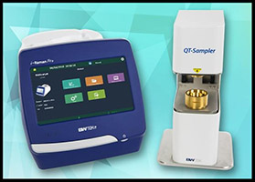
Powered by B&W Tek’s award-winning STRaman™ technology, the QTRam features a portable Raman system with 21 CFR Part 11 compliant software on an embedded tablet computer for blend & content uniformity, quantitative analysis, and at-line analysis for process monitoring & final release testing.

About B&W TEK
B&W Tek is an advanced instrumentation company producing optical spectroscopy and laser instrumentation, as well as laboratory, portable and handheld Raman systems. We provide spectroscopy and laser solutions for the pharmaceutical, biomedical, physical, chemical, LED lighting and research communities. Originally established as a producer of green lasers in 1997, we’ve grown into an industry-leading, total solutions provider; coupling our core technologies with custom design and manufacturing capabilities.

Wireless Test Solution

Next Generation Solutions for Wireless Communication Systems

ATE Industry’s First Fully Integrated Single Module with 4-unique RF Vector Signal Generators and Analyzers (WLS32-A Module)

  • High-Performance VSG and VSA Instrumentations Supporting Complex Modulation Densities up to 80MHz Bandwidth
  • Fast Test Times Achieved with Fast Settling Synthesizer Switching
  • Highest Industry RF Port Density (32 per module and scaleable to 128) for Today’s and Tomorrow’s Multi-DUT MIMO and Transceiver Applications (WLS32-A)
  • For Low Cost small system, Half RF Port Density (WLS16-A)
  • High-Speed & High Carrier to Noise Ratio Synthesizer Modes to Address Production and Characterization Solutions
  • Integrated Low-Noise, Low-Jitter Programmable Reference Signal Generator for Crystal (TCXO) Reference
  • Internal Highly Linear 2-tone Combiner to Produce > +28dBm (@2.2GHz, -12dBm) Output IP3 to Device
  • Lowest COT Achieved with Quad-DUT Native Capability (Parallel Source and Measure)
img_t2000_0006_en

CMOS Image Sensor Test Solution

The T2000 CMOS Image Sensor Test Solution is a single solution for evaluation and production testing of advanced CMOS image sensors with high-speed interfaces up to 3 Gbps. This highly parallel system uses concurrent hardware operation, a fast IP engine, a high-speed bus and reduced shot counts to provide users with one of the industry’s lowest cost of test.

Flexible support for multifunction image sensors

CMOS image sensors are now incorporating functions such as AD/DA and other SoC circuits. With its modular architecture, the T2000 can achieve the optimal configuration to test these complex devices while delivering low cost of test.
The system’s high-speed image-capture interface supports a variety of CMOS image sensors including mobile, DSC, DSLR, CAM and industrial CIS. In addition, the large dual-bank memory module enables simultaneous storage and transfer of data to the image-processing engine, minimizing test times.


The system is available in two versions:

1.2-Gbps CMOS Image Capture (1.2GICAP) Module

  • Image Capture input:
    Serial data: 1.2 Gbps, 4 lanes x 4 channels
    ・1.2 Gbps for MIPI D-PHY and sync code mode (Custom S-LVDS)
    Parallel data: 200 M pixels/s, 16 bits x 4 channels
  • Capture memory: 128 M pixels x 2 banks
    Maximum frame averaging number up to 256 frames (hardware averaging)

3-Gbps CMOS Image Capture (3GICAP) Module

  • Image Capture input:
    Serial data: 1.2 Gbps, 4 lanes x 4 channels
    ? 1.2 Gbps for MIPI D-PHY and sync code mode ?Custom S-LVDS?
    Parallel data: 200 M pixels/s, 16 bits x 4 channels
  • Capture memory: 128 M pixels x 2 banks
    Maximum frame averaging number up to 256 frames (hardware averaging)

Faster Processing for Higher Throughput

With its high-speed quad processors for image-capture data analysis, Advantest’s new image processor engine (IPE2) significantly reduces test times, especially for higher pixel CMOS image sensors.

Light Source and Large User Area Delivers Higher Parallelism
at a Low Cost of Test

img_t2000_0007_en

The module’s ultra-high-volume, simultaneous measurement capability enables uniquely high productivity and a significant cost savings for image-sensor testing. Most importantly, the optimized, uniform light source and large user area enable highly parallel testing of ultra-high-density and high-performance devices.

  • 440 mm probe card and 2048-channel frog unit (pogo interface)

THE USE OF ASYLUM TECHNOLOGY

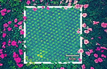
Topological structures in multiferroic materials have recently received considerable attention because of their potential use as nanoscale functional elements. Their reduced size in conjunction with exotic arrangement of the ferroic order parameter and potential order parameter coupling allows for emergent and unexplored phenomena in condensed matter and functional materials systems. This will lead to exciting new fundamental discoveries as well as application concepts that exploit their response to external stimuli such as mechanical strain, electric and magnetic fields. In this review we capture the current development of this rapidly moving field with specific emphasis on key achievements that have cast light on how such topological structures in multiferroic materials systems can be exploited for use in complex oxide nanoelectronics and spintronics.

  1. Introduction

Topological defects play important roles in nature. They are found in fields as diverse as cosmology, [ 1] particle physics, superfluidity, liquid crystals, and metallurgy, manifesting themselves as e.g. screw/edge-dislocations in liquid crystals, [ 2] magnetic flux tubes in superconductors, [ 3] and vortices in superfl uids [ 4] etc. The theory of topological defects, as applicable to condensed matter physics, dates back to the seminal work of Mermin in 1979. [ 5] In a non-uniform ordered medium (i.e., media that can be described by a function f( r ) which assigns an order parameter to every point in that space), topological defects are those regions including points, lines and surfaces where the order parameter ceases to vary continuously, forming regions of lower dimensionality.

At the same time, the possible values that the order parameter can take constitute the order parameter space. For example, the order parameter space for planar spins can be taken as a unit vector that can point in any direction in a plane, i.e., the space is a circle. This allows for mapping of a closed contour of the order …….. Read More from PDF
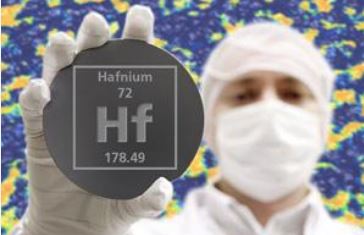
pdf