
Continued reduction in the size of transistor devices has lead to the replacement of silicon oxide by hafnium oxide as gate oxide in MOSFETS in the mid-2000s [i]. Hafnium oxide, a high-k dielectric material, is one of the few binary oxides that are thermodynamically stable with silicon. It can thus be naturally integrated in logic and memory devices. Intel, for example, announced in 2007 the incorporation of hafnium-based high-k metal gates in their processors [ii]. This new transistor formulation promised to be lower in power consumption with reduced electricity leaks, while delivering performance that comes with downscaling.
In 2011, the ferroelectricity of hafnium oxide was reported [iii]. All bulk phases of hafnium oxide have centrosymmentric crystal structures, and therefore do not exhibit ferroelectricity. Hafnium oxide is monoclinic at room temperature and tetragonal above 2050 K. However, when doped with silicon oxide during the formation of thin films under mechanical encapsulation (“capping”), hafnium oxide forms crystalline phases that are non-centrosymmetric, and therefore expected to be ferroelectric [iv]. This ferroelectric phase is orthorhombic, and is formed by the inhibition of the tetragonal to monoclinic transition by mechanical confinement. Ferroelectricity of hafnium oxide potentially leads to interesting devices taking advantage of silicon/ferroelectric junctions. Ferroelectric transistors (FeFETS), for example, show promise as ultra-fast, low-power non-volatile memory, that may eventually compete with current flash technology [v, vi, vii].
A challenge in the characterization of hafnium oxide thin films is the weak piezoelectric response, a property of ferroelectric materials. Piezoresponse force microscopy (PFM) often needs to be done at the contact resonance frequency to take advantage of resonance enhancement of the signal [viii]. The frequency of the contact resonance shifts, however, and can introduce topographic crosstalk that can obscure the piezoelectric response.
Asylum Research’s proprietary Dual Amplitude Resonance Tracking or DART™ modetracks contact resonance shifts, thus minimizing the influence of topography on the measurement. Here are some examples of DART™-PFM images of Si:HfO2 thin films clearly showing poled piezoelectric domains. The sample is a 10 nm thin film in its initial state after crystallization, before wake-up cycling. These data were taken during the installation of a customer’s new Cypher S system.
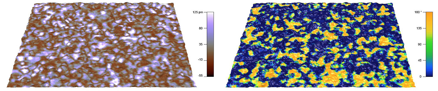
DART amplitude (left) and phase (right) data overlaid on topographic surface of 10 nm Si:HfO2 thin film (3 µm scan size).
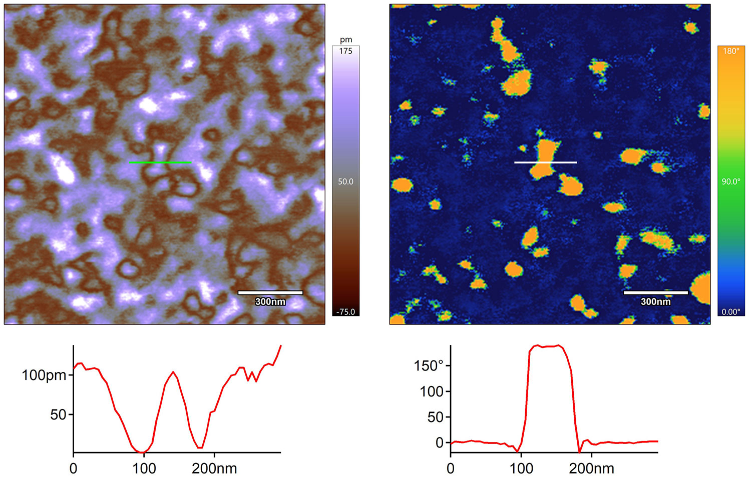
DART amplitude (left) and phase (right) images of 10 nm Si:HfO2 thin film (1.5 µm scan size), with line sections across piezoelectric domains of opposite polarity.
References:
[i] Zhu, H., C. Tang, L. R. C. Fonseca, and R. Ramprasad. “Recent progress in ab initio simulations of hafnia-based gate stacks.” Journal of Materials Science 47, no. 21 (2012): 7399-7416.
[ii] Intel News Release: “Intel’s Fundamental Advance in Transistor Design Extends Moore’s Law, Computing Performance: Sixteen Eco-Friendly, Faster and ‘Cooler’ Chips Incorporate 45nm Hafnium-Based High-k Metal Gate Transistors” (https://www.intel.com/pressroom/archive/releases/2007/20071111comp.htm)
[iii] Böscke, T. S., J. Müller, D. Bräuhaus, U. Schröder, and U. Böttger. “Ferroelectricity in hafnium oxide thin films.” Applied Physics Letters 99, no. 10 (2011): 102903.[iv] Polakowski, Patrick, and Johannes Müller. “Ferroelectricity in undoped hafnium oxide.” Applied Physics Letters 106, no. 23 (2015): 232905.
[v] NamLab (Nanoelectronic Materials Laboratory) Website: “Hafnium Oxide Based Ferroelectric Memory (http://www.namlab.de/research/reconfigurable-devices/hafnium-oxide-based-ferroelectric-memory)
References:
[i] Zhu, H., C. Tang, L. R. C. Fonseca, and R. Ramprasad. “Recent progress in ab initio simulations of hafnia-based gate stacks.” Journal of Materials Science 47, no. 21 (2012): 7399-7416.
[ii] Intel News Release: “Intel’s Fundamental Advance in Transistor Design Extends Moore’s Law, Computing Performance: Sixteen Eco-Friendly, Faster and ‘Cooler’ Chips Incorporate 45nm Hafnium-Based High-k Metal Gate Transistors” (https://www.intel.com/pressroom/archive/releases/2007/20071111comp.htm)
[iii] Böscke, T. S., J. Müller, D. Bräuhaus, U. Schröder, and U. Böttger. “Ferroelectricity in hafnium oxide thin films.” Applied Physics Letters 99, no. 10 (2011): 102903.
[iv] Polakowski, Patrick, and Johannes Müller. “Ferroelectricity in undoped hafnium oxide.” Applied Physics Letters 106, no. 23 (2015): 232905.
[v] NamLab (Nanoelectronic Materials Laboratory) Website: “Hafnium Oxide Based Ferroelectric Memory (http://www.namlab.de/research/reconfigurable-devices/hafnium-oxide-based-ferroelectric-memory)