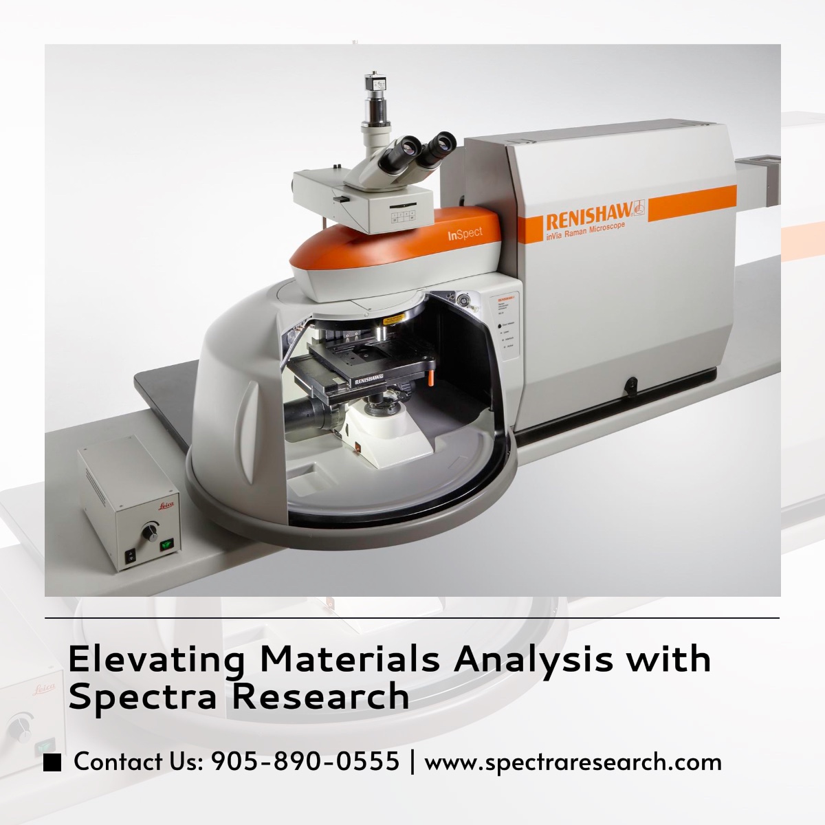
Ceramic 3D Printing & Advanced Filament Extrusion Tour in Canada
Join SRC, 3DCERAM, and 3devo for a free on-site event series featuring expert talks, live instrument demonstrations, and application discussions on ceramic additive manufacturing, filament development, and advanced materials workflows.
Time: 9:00 AM ET – 1:45 PM ET
|
|
|
See additive manufacturing workflows beyond slides:
This tour is designed for researchers, engineers, and technical teams who want to move beyond product overviews and understand how ceramic 3D printing and filament extrusion fit into real development workflows. The program connects scientific challenges with process capability, materials behavior, instrument design, and practical application discussions led by SRC and supplier specialists.
Questions this event helps address
|
Why this matters with SRC
|
Tour Details:
One event series, three Canadian stops. Each session includes technical talks, live demos, networking, and direct conversations with SRC, 3DCERAM, and 3devo. Replace the placeholder registration links below with your final event URLs.
| Montreal | Ottawa | Hamilton |
École de Technologie Supérieure (ETS):
|
University of Ottawa, STEM Complex:
|
McMaster Manufacturing Research Institute:
|
Event Agenda:
Each stop follows the same half-day format, combining expert presentations with networking and hands-on technology exposure.
| 9:00 AM – 9:15 AM | Introduction by SRC |
| 9:15 AM – 10:00 AM | Jose’s talk – From Material Idea to Controlled Application: A Practical Approach to Filament Development and Q&A |
| 10:00 AM – 10:15 AM |
Coffee Break |
|
10:15 AM – 11:00 AM
|
Rouslan’s talk – Ceramic 3d printing with Multi-Additive Technology printer: capabilities, materials and applications and O&A |
|
11:00 AM – 12:00 PM
|
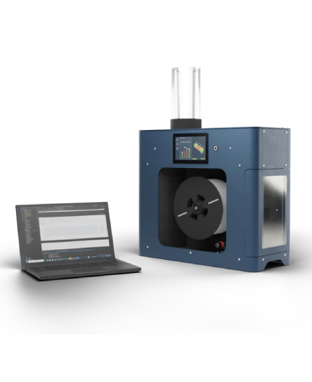
3devo Demo – Filament Maker TWO |
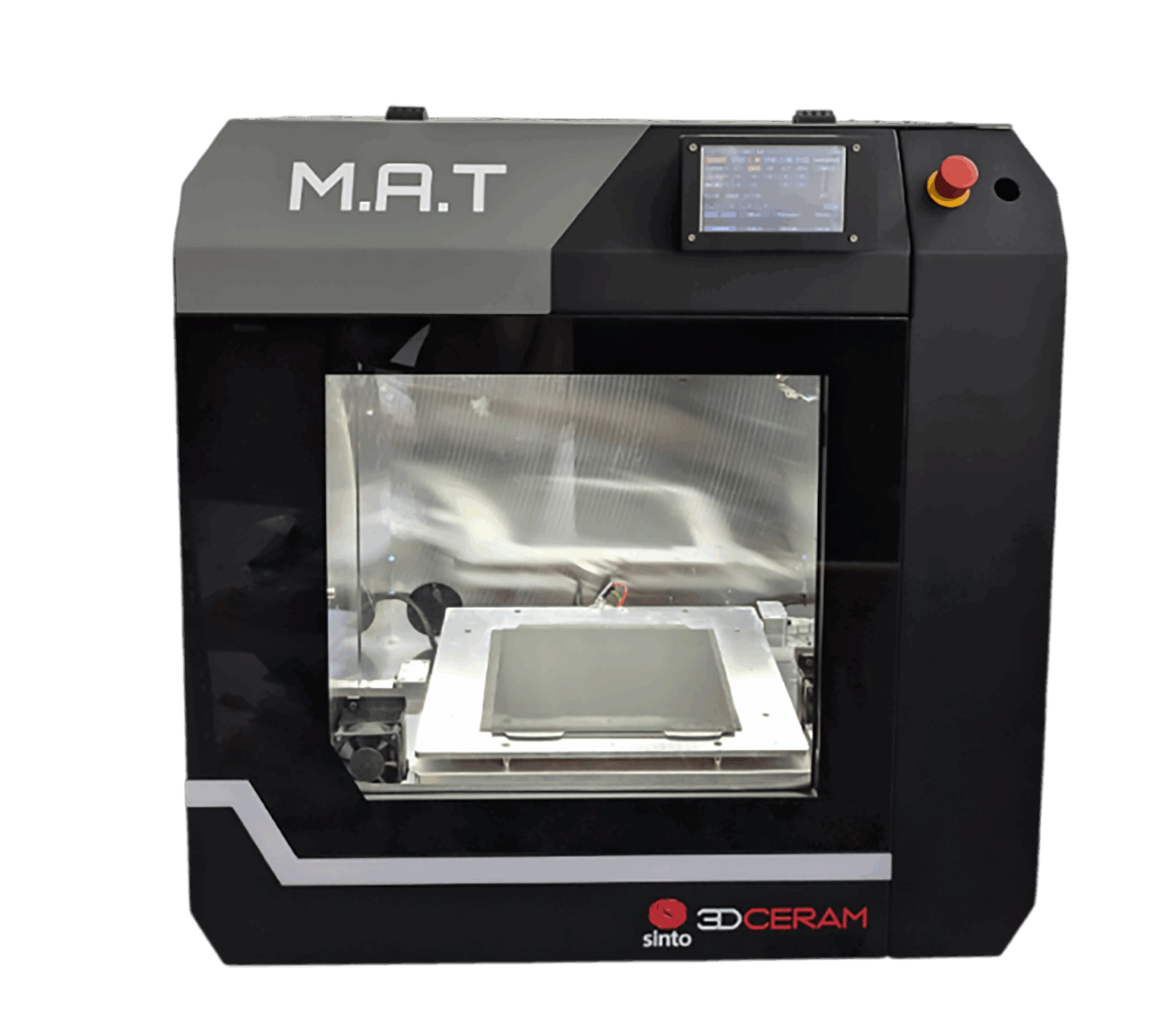
| 12:00 PM – 12:45 PM | 3DCERAM Demo – M.A.T. (Multi Additive Technology) |
| 12:45 PM – 1:45 PM |
Lunch and Discussions |
Featured Presentations:
Two supplier-led sessions designed for technical audiences evaluating materials, process capability, and additive manufacturing workflow fit.
 |
 |
Rouslan Svintsitski | Area Sales Manager, 3DCERAM Sinto SAS |
José Rui Capitão | Application Specialist, 3devo B.V. |
Rouslan Svintsitski brings more than 30 years of experience in ceramic processes and technologies, spanning technical ceramics, extrusion, and international business development in ceramic 3D printing. His recent work has focused on advanced ceramic materials and additive manufacturing workflows for demanding applications in investment casting, aerospace, and defense.
Ceramic 3D Printing with Multi-Additive Technology Printer: Capabilities, Materials and ApplicationsThis session explores extrusion-based ceramic additive manufacturing with a focus on fused filament fabrication for advanced ceramics. It examines why extrusion-based approaches can be especially relevant for dark ceramics such as silicon carbide, where optical limitations can make other ceramic AM routes more challenging.
|
José supports customers worldwide in material selection, material research, and recycling-oriented workflows using advanced extrusion technologies. He combines technical engineering expertise with customer-focused problem solving in material innovation environments.
Advanced Filament Extrusion: Turning Materials into Filament through Tools, Theory, and InnovationThis session provides a structured look at how raw materials are transformed into high-quality filament through controlled extrusion workflows. It covers key equipment, extrusion theory, material behavior, process parameters, and strategies for new material development.
|
Live Instrument Demonstrations:
The tour is designed to bring prospects into the room with the equipment. Attendees will see the instruments, discuss workflow details, and connect process capability to their own application requirements.
 |
 |
3DCERAM M.A.T. (Multi Additive Technology)See how extrusion-based additive manufacturing can support ceramic and metal part development using a platform designed to combine multiple deposition methods with integrated green machining. The session will center on capabilities relevant to complex ceramic geometries, dark ceramic processing, and post-print workflow considerations.
|
3devo Filament Maker TWOSee a controlled filament extrusion workflow designed for material validation, process development, and repeatable filament production. This demonstration is especially relevant for teams developing new materials, refining process settings, or connecting filament performance to downstream additive manufacturing workflows.
|
Who Should Attend:
This event is designed for Canadian technical audiences working across material development, process engineering, and additive manufacturing.
Research & Academic Teams
|
Government & Innovation Labs
|
Industrial R&D
|