
That may not be how the saying goes, but, just like the brilliant blooms each spring, I continue to be captivated by the view that scanning probe microscopy—well, nanoscopy—gives us into ultra-small surface structure. Perhaps no scanning probe technique remains more mesmerizing to me than scanning tunneling microscopy (STM). That’s the Nobel-prize-worthy invention [i] where we raster an atomically sharp stylus back and forth at a distance of a few angstroms from a surface and measure fractions of nanoamps of current without destroying the tip. STM is one of those rare instances where we get to see and use a quantum mechanical process—electron tunneling—in the macro world. And it still defies belief to some extent: anyone who has even sniffed the quantum mechanics kool-aid might balk at the notion that we could control the tip-sample distance to within an atomic radii AND measure a current that exponentially depends on that distance (see Figure 1).
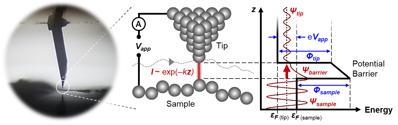
Figure 1. Scanning Tunneling Microscopy in the Cypher ES. (Left) A magnified view of a STM probe approaching the HOPG surface inside the Cypher ES. (Right) A schematic showing some of the principles of electron tunneling, where Vapp is applied bias, e is the elementary charge, I is current, z is vertical distance, εF is Fermi level, Φ is work function, Ψ is the electron wave function, and k ~ Φ½ is the characteristic inverse decay length. Assuming Φ ≈ 5 eV, each 1 Å change in z causes an order of magnitude change in current, yielding extreme z sensitivity!
It turns out that the STM does work, at least in some cases, and much of that is owed to improvements in instrument precision: fine position control with piezoelectric crystals [ii], noise reduction by engineering a smaller sample-tip mechanical loop such as that found in Asylum’s Cypher line of instruments, and most recently, ultra-low-noise current amplifiers enabling tiny tunneling current setpoints. All this conspires to mean that STM is routinely achievable in a range of conditions with detectable currents below 1 pA. Traditionally, high resolution STM imaging is difficult in ambient and liquid conditions, with the most impressive images arguably coming from ultra-high vacuum measurements at ultra-low temperatures. Seeing as our Cypher instruments are designed for stable operation in ambient and liquid conditions, it made sense to work on extending the low-current range for STM on this platform. So, we installed one of these new ultra-low-current amplifiers on a Cypher ES here at Asylum.
I was then called upon separately by Professor Kerry W. Hipps (Washington State University) and Professor Michael D. Hopkins (University of Chicago) with a challenge to obtain low-current-STM images of self-assembled 2D metalloporphyrin crystals on HOPG at ambient conditions. The conventional sample preparation here is straightforward: ~1 μL of a solution of Cobalt or Nickel octaethylporphyrin (CoOEP or NiOEP, respectively) in phenyloctane deposited on freshly-cleaved HOPG allows metalloporphyrins to spontaneously form the desired conformal lattice through π-π interactions with the graphitic carbon, while the phenyloctane remains on the surface.
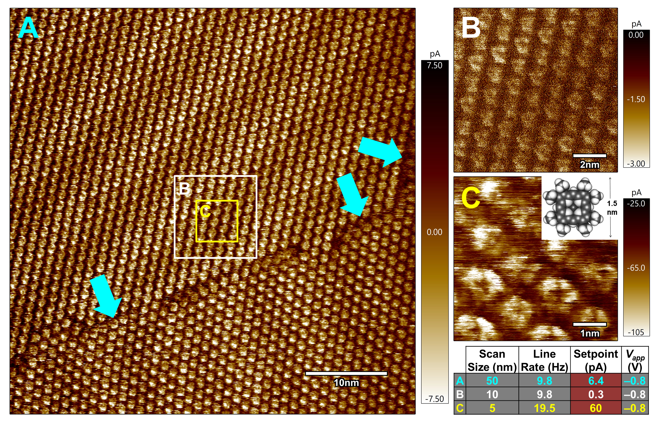
Figure 2. Tip current images of the 2D lattice of NiOEP on HOPG. (A) Survey scan (flattened) showing the NiOEP grain boundary (blue arrows), zoom regions, and moiré pattern. (B) Zoom region imaged at 300 fA setpoint. (C) Zoom region showing sub-nm molecular resolution. Inset: the CPK molecular model of NiOEP (adapted from ref. [iii]).
Prof. Hopkins sent a solution of NiOEP, while Prof. Hipps sent a solution of CoOEP, and I followed the simple deposition procedure above to form the 2D lattices. With our house-made 80/20 Pt/Ir STM probes (available from our Probe Store) and logarithmic current feedback, I was able to get stunning resolution at a variety of imaging conditions for both samples. As you can see in Figure 2, I was able to find a grain boundary in the lattice of NiOEP molecules. I also managed to resolve the lattice at a remarkable 300 fA setpoint (that’s a measly ~2 million electrons/second) and obtain sub-nanometer molecular resolution of the porphyrin rings! In Figure 3, the CoOEP lattice is also readily apparent, as are the porphyrin ring structures. For those images we changed the current and applied voltage and cranked up the integral gain to resolve the lattice in the height channel. Many thanks to my colleague Keith Jones for help with those images. All of these data were acquired at ambient conditions in air, with no particularly involved cleaning or extra sample preparation steps.
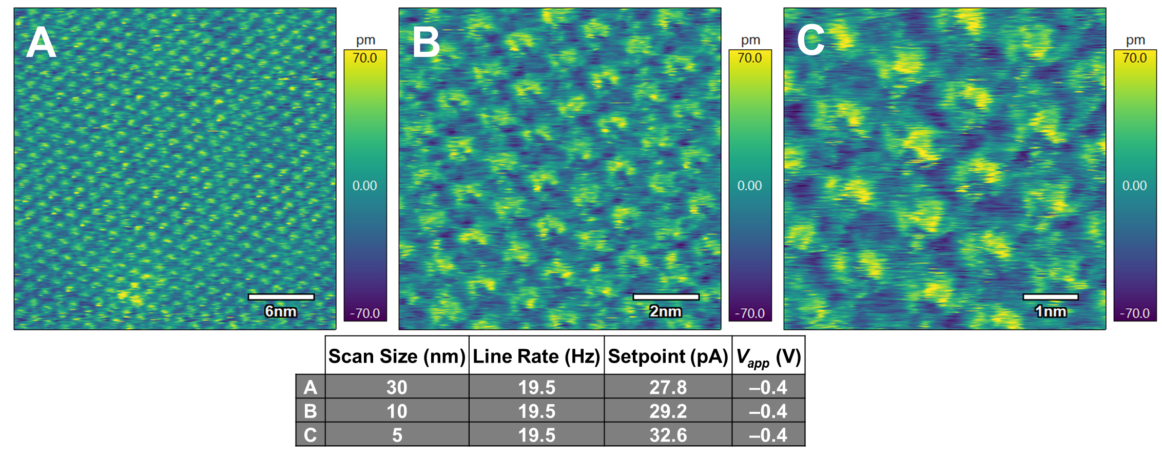
Figure 3. Tip height images of the 2D lattice of CoOEP on HOPG. (A) Survey scan showing the CoOEP 2D lattice. (B) Zoomed view showing sub-molecular structure. (C) Further zoom showing sub-nm molecular topographic resolution.
All told, these images might be better to look at than flowers anyway—especially if you choose the right color palette! I’m looking forward to combining this new extraordinary imaging with other techniques, so stay tuned to see what we come up with.
Happy Springtime,
Nate
References
[i] G. Binnig, H. Rohrer, Ch. Gerber, and E. Weibel, Applied Physics Letters 40 (1982), 178-180, https://aip.scitation.org/doi/pdf/10.1063/1.92999.
[ii] (a) G. Binnig et al., Piezo drive with coarse and fine adjustment, IBM Technical Disclosure Bulletin 22(7) (1979), 2897-2898, New York, US; (b) See also V. B. Elings, J. A. Gurley, Positioning device for a scanning tunneling microscope, US Patent 4,871,938 (1988) and its cited and citing patents: https://patents.google.com/patent/US4871938A/en.
[iii] L. Scudiero, D. E. Barlow, K. W. Hipps J. Phys. Chem. B, 2002, 106 (5), pp 996–1003. https://pubs.acs.org/doi/abs/10.1021/jp012436m