
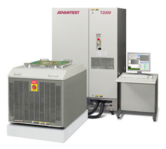
High-performance, low-cost SoC test solution optimized for high-volume manufacturing of today’s complex consumer devices.
Drastic reductions in cost-of-test
 * Based on ADVANTEST COST model
Offering increased parallelism and high-speed digital and analog modules, the T2000 test system provides dramatic reductions in cost-of-test which is critical for digital consumer market with:
- A compact ATE footprint (LSMF)
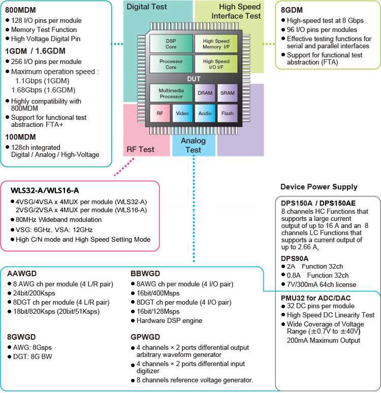
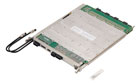
- A digital module (1GDM / 1.6GDM) which offers high density (256 channels) and low cost
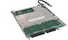
- Two analog modules (AAWGD, BBWGD) with 2x the channel counts of alternative solutions
- A DC test solution (PMU32), which provides 32 high accuracy channels per module, for ADC/DAC and other DC test challenges
Combining these and other features enables twice the throughput and half the cost-of-test.
State-of-the-art, feature-rich capabilities
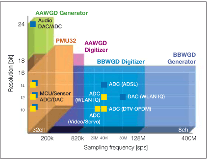 Analog modules provide broad coverage
The T2000 test system responds to the needs of the digital consumer market’s ever-increasing demand for product versatility and sophisticated functionality with:
- Multi Time Domain functionality for testing multiple frequency domains simultaneously
- 1GDM / 1.6GDM realizes low cost of test by high parallel testing
- DSP90A module supports 64ch device power supply by high density mounting
- Analog modules (AAWGD, BBWGD) providing full-spec test, providing coverage from high-performance audio to video and baseband
- 8GWGD which covers wide frequency and high speed sampling Analog tests
- PMU32 module capable handling a broad spectrum of precision test including ADC/DAC linearity
- GPWGD realizes full spec test from high spec audio to video frequency
- 8GDM corresponds to high speed interface device testing
- 800MDM which provides measurement functionality necessary to validate source-synchronous interfaces, such as for DDR2
Combined with newly developed test modules and LSMF, T2000 provides optimized test solution for fast growing consumer devices.
Digital Consumer Solution
Various modules for your digital consumer device testing:
LSMF
- Test Head Slots: 26 slots
- MF Size: 800(W) x 1050(D) x 1600(H)mm
- Maximum Site Controller Count: 4
MPU Solution
T2000 Test System —
An MPU Solution that provides a technical edge for testing high-end MPUs, high-speed buses and communication interfaces. It is the ultimate solution for continual, rapid advancements in MPU devices.
T2000 Offers Scalable Solutions for Demanding MPU Testing
- High-speed Bus and Communication Interface Testing by High- speed Differential Driver/Comparator sources
- Clock vs. Data Synchronous Testing of High-speed Bus by Source Synchronous Functionality
- Concurrent Test by Multi Time Domains
- High-speed MPU Testing by High-current Device Power Supply of 150A Module
- Independent Flow Control by Multi-site Controllers
User-Friendly Environment by Windows
T2000 Operating System is easy-to-use with a wide variety of choices of application archives. For evaluation and silicon debug characterization, tools such as Wave Tool (Logic Analyzer, Oscilloscope), Shmoo, Margin, and Pattern Editor speed up time to yield. Additionally, the simulation environment is transparent to the operational implementation allowing fully off-line program development.
Wireless Test Solution
Next Generation Solutions for Wireless Communication Systems
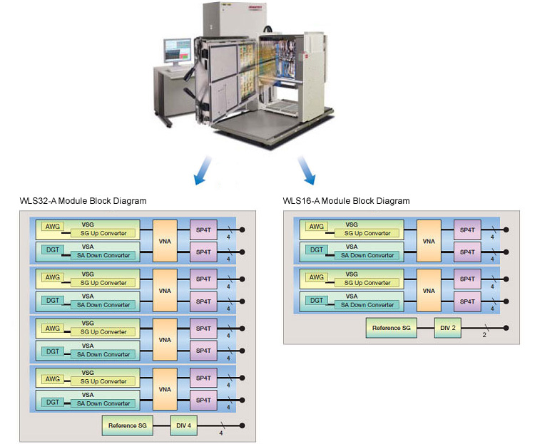
ATE Industry’s First Fully Integrated Single Module with 4-unique RF Vector Signal Generators and Analyzers (WLS32-A Module)
- High-Performance VSG and VSA Instrumentations Supporting Complex Modulation Densities up to 80MHz Bandwidth
- Fast Test Times Achieved with Fast Settling Synthesizer Switching
- Highest Industry RF Port Density (32 per module and scaleable to 128) for Today’s and Tomorrow’s Multi-DUT MIMO and Transceiver Applications (WLS32-A)
- For Low Cost small system, Half RF Port Density (WLS16-A)
- High-Speed & High Carrier to Noise Ratio Synthesizer Modes to Address Production and Characterization Solutions
- Integrated Low-Noise, Low-Jitter Programmable Reference Signal Generator for Crystal (TCXO) Reference
- Internal Highly Linear 2-tone Combiner to Produce > +28dBm (@2.2GHz, -12dBm) Output IP3 to Device
- Lowest COT Achieved with Quad-DUT Native Capability (Parallel Source and Measure)
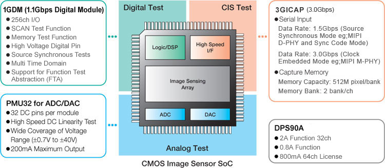
CMOS Image Sensor Test Solution
The T2000 CMOS Image Sensor Test Solution is a single solution for evaluation and production testing of advanced CMOS image sensors with high-speed interfaces up to 3 Gbps. This highly parallel system uses concurrent hardware operation, a fast IP engine, a high-speed bus and reduced shot counts to provide users with one of the industry’s lowest cost of test.
Flexible support for multifunction image sensors
CMOS image sensors are now incorporating functions such as AD/DA and other SoC circuits. With its modular architecture, the T2000 can achieve the optimal configuration to test these complex devices while delivering low cost of test.
The system’s high-speed image-capture interface supports a variety of CMOS image sensors including mobile, DSC, DSLR, CAM and industrial CIS. In addition, the large dual-bank memory module enables simultaneous storage and transfer of data to the image-processing engine, minimizing test times.
The system is available in two versions:
1.2-Gbps CMOS Image Capture (1.2GICAP) Module
- Image Capture input:
Serial data: 1.2 Gbps, 4 lanes x 4 channels
・1.2 Gbps for MIPI D-PHY and sync code mode (Custom S-LVDS)
Parallel data: 200 M pixels/s, 16 bits x 4 channels - Capture memory: 128 M pixels x 2 banks
Maximum frame averaging number up to 256 frames (hardware averaging)
3-Gbps CMOS Image Capture (3GICAP) Module
- Image Capture input:
Serial data: 1.2 Gbps, 4 lanes x 4 channels
? 1.2 Gbps for MIPI D-PHY and sync code mode ?Custom S-LVDS?
Parallel data: 200 M pixels/s, 16 bits x 4 channels - Capture memory: 128 M pixels x 2 banks
Maximum frame averaging number up to 256 frames (hardware averaging)
Faster Processing for Higher Throughput
With its high-speed quad processors for image-capture data analysis, Advantest’s new image processor engine (IPE2) significantly reduces test times, especially for higher pixel CMOS image sensors.
Light Source and Large User Area Delivers Higher Parallelism
at a Low Cost of Test
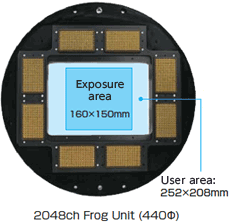
The module’s ultra-high-volume, simultaneous measurement capability enables uniquely high productivity and a significant cost savings for image-sensor testing. Most importantly, the optimized, uniform light source and large user area enable highly parallel testing of ultra-high-density and high-performance devices.
- 440 mm probe card and 2048-channel frog unit (pogo interface)
T2000 module configuration for CMOS image sensor testing
Scalable System Configuration
| Value Package | Standard Package | Performance Package | |
|---|---|---|---|
 |
 |
 |
|
| Parallel Test | 16 | 32 | Beyond 32 |
| Main Frame | LSMF | LSMF | LSMF+EXMF |
| Test Head | 13 slot | 46 slot | 46 slot |
Integrated Power Device Test Solution
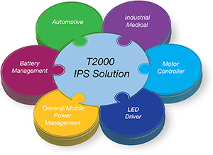
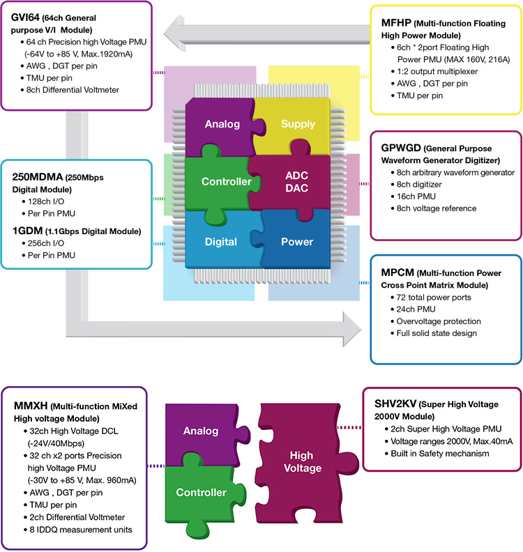
Advantest’s T2000 Integrated Power Device Test Solution (IPS) is a high-performance, high-throughput tester for mixed-signal devices used in applications ranging from automotive ASSP/ASIC, Analog Power ICs that power management semiconductors (PMICs) for high-volume consumer electronics, communication products and industrial usage. With the added advantage of our available modules such as the MMXH, MFHP, MPCM, and GVI64 as well as other T2000 modules, the T2000 system is designed to perform massively parallel testing at a low cost of test.
Based on Advantest’s more than 27 years of experience in producing analog test solutions, the T2000 system with IPS delivers industry-leading results and award-winning customer satisfaction.
Setting a New Standard
This system raises the bar for ATE performance with its wide range of capabilities:
- Wide coverage for testing PMICs, LED Driver ICs, wireless/Industrial applications, Li-Ion battery monitor IC, high-voltage Automotive ASSP/ASIC, etc.
- Enhanced test efficiency using per-channel time measurements
- Highly parallel testing through load board simplicity and matrix functionality
- Increased throughput with pattern-controlled test conditions
- Best-in-class performance, including fast range switching hardware, fast switching relays and concurrent hardware operation
- Low cost-of-test with unprecedented channel density and parallelism
- High flexibility and ease-of-use due to a multi-functional mixed-signal architecture
- Simplified coding enabled by the EASE software package, which provides a user-friendly environment for developing re-usable coding and fast debugging
Optimized Module for Power Mixed Signal Test
IGBT Test Solution
The T2000 also enables highly productive testing of insulated-gate bipolar transistors (IGBT):
- Equipped for AC+DC x 2 DUT testing
- High-speed breaker improves yield while also protecting both the wafer probe and the stage from high temperatures.
- Low-inductance design allows high-speed switch testing
- Ability to be used in both engineering and production environments, including compatibility with various software tools for easy code development and debugging
Integrated Massive parallel Test Solution
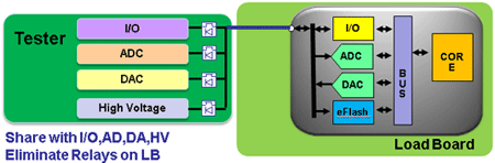
T2000 architecture supports high parallelism and high MSE
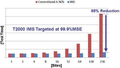
T2000 IMS Architecture
Especially for MCU, SmartCard, RFID devices, we are providing Integrated Massive parallel Test Solution (IMS). It could achieve highest MSE even large dut count for parallel testing.
Key features
- Unified pin architecture reduce relay on PB dramatically.
- Great MSE
- Cost Effective solution
EPP (Enhanced Performance Package)
The EP Package is a solution offering stronger and more diverse functionality, along with low test cost and shorter development time for testing programs of SoC devices, which Time to Volume is the key.
Three Expanded Functions
The new EP Package expands three functions to the current available T2000.
- Low-Cost Multi-Site CPU Configuration
Multi-site CPU configuration offers multi-site CPU functionality with cost in-line with that of traditional single-site CPUs, with high throughput and multi-user environment. - Concurrent Test
Concurrent test enables simultaneous execution of multiple test flows, as well as faster development of shorter-time testing programs, through these it contributes to lower Cost of Test and shorter Time to Market. - Functional Test Abstraction (FTA)
FTA makes execution of system-level design verification programs on ATE at the protocol level possible, shortening Time to Market.
Rich Functionality by High Density Mounting
The three expanded functions, together with new high-density modules, bring more diverse functionality while using fewer modules. This makes incorporating up to 8,192 digital channels possible, enabling over twice the parallel testing capacity of our earlier model.
- 1.6GDM
The 1.6GDM is compatible with its predecessor module while offering increased throughput and reliability. It can communicate with the DUTs in each device’s protocol language and, through FTA-Elink, run Verilog code.
- DPS90A
DPS90A incorporates 64 DPS channels, and supports parallel testing of SoC devices, for which power supplies are becoming ever more numerous.
- GPWGD
GPWGD features wideband, high-sampling rate testing, and offers audio, video and baseband applications in a single module.
- DPS150AE
DPS150AE can handle the load requirements for highly accurate testing of both high-current and low-voltage semiconductors. The module improves the capabilities of the T2000 platform in performing high-throughput, multi-site testing of targeted devices with the lowest cost of test.
Key Features
- EP Package
Multi-site CPU:max. 8 sites
Module support:max. 52
Bus speed:4Gbps
Supports concurrent test and functional test abstraction
(with TSC4+SGM208+CUTI configuration) - 1GDM: 1Gbps Digital Module
Channels:256 per module
Max. data rate:1.1Gbps
Pattern memory:256MW - 1.6GDM: 1.6Gbps Digital Module
Channels:256 per module
Max. data rate:1.68Gbps
Pattern memory:256MW - DPS90A: Device Power Supply 90A
Power source: 2A x 32 channels, 0.8A x 32 channels Supports high-accuracy ISVM - GPWGD: General Purpose Waveform Generator and Digitizer
Waveform Generators:8 (1Msps/50Msps)
Digitizers:8 (1Msps/50Msps)
Supports DC linearity test - DPS150AE: Device Power Supply 150A
Power source:
High Current function – 16A×8 channels
Low Current function – 2.66A×8 channels