FREE WEBINAR FROM ASYLUM RESEARCH on Application of Atomic Force Microscopy in Virology Research

WEBINAR DATE

Wednesday August 12, 2020
12:00 PM – 1:00 PM EDT

Atomic Force Microscopy has found broad use in the biological sciences. It is an indispensable tool for both high resolution imaging of individual molecules, cells, tissues, viruses and biomaterials. Since AFM is also relatively non-destructive and requires minimal sample preparation (i.e. no coating/fixing/labeling), it is ideally suited to visualize
dynamic biomolecular processes at the nanoscale.
We will present relevant data to illustrate the potential of Asylum Research’s AFMs in virus research.


Sophia Hohlbauch, Senior Biological Applications Scientist @Asylum Research
Sophia Hohlbauch has over 20 years of AFM experience specializing in the life sciences. She is currently a Senior Biological Applications Scientist at Asylum Research and previously held a similar position at Digital Instruments/Veeco. She has presented on AFM topics at numerous biology and AFM meetings worldwide. Her background is biology, receiving Bachelor’s and Master’s degrees in Marine Biology from the University of California, Santa Barbara.

McGill University AFM Summer School and Workshop

McGill University AFM Summer School and Workshop
June 6-7, 2018

Topics Increase Your AFM Knowledge
Are you looking to better understand the AFM techniques that are used in your research? Asylum Research invites you to the McGill AFM Summer School and Workshop which includes lectures and hands-on demonstrations from leading researchers and experts in the field.

• Video-Rate AFM with the Asylum Research Cypher VRS
• Organic control of biomineral nanostructure
• Time-resolved, ultra fast AFM imaging
• High resolution electrochemistry for energy storage applications
• Nanomechanical measurements

Hands-on demonstration labs will complement the lectures. It’s an excellent opportunity to get tips and tricks on AFM operation, and to see video-rate AFM in action.

Speakers
Dr. Peter Grütter, Chair, Dept. of Physics, McGill University
Dr. Marc D. McKee, Dept. of Anatomy and Cell Biology, McGill University
Sophia Hohlbauch & Marta Kocun, Applications Scientists, Asylum Research
Mayur Savla, US Technical Sales, Asylum Research

Registration
$50 USD which includes lectures, labs, lunches for both days and Happy Hour on June 6.

Contact Us

Serge Dandache

Spectra Research Corporation
3585 Laird Rd., Unit 15 & 16,
L5L 5Z8 Mississauga
Ontario
Canada.

Phone 905-890-0555

Toll Free : 1-866-753-4433
Fax 905-890-1959

Applications of the NanoRack™ Sample Stretching Stage to a Commercial Impact Copolymer

Dalia G. Yablon and Andy H. Tsou, ExxonMobil Research and Engineering, Clinton, NJ

A commercial impact copolymer (ICP), amulticomponent material typically used inautomotive and appliance applications where a balance of stiffness and toughness is needed, was studied with the NanoRack™ Sample Stretching Stage accessory on the MFP-3D™Atomic Force Microscope to investigate material deformation and interface adhesion as a function of tensile stress. Effects of deformation were observed within both the polypropylene  and ethylene-propylene components, as well as at the interface between the two materials. There are no other direct measurement methods available to determine interfacial adhesive strength of polymer blends, and so AFM investigations of micro-domain deformation such as the one described here could be used ultimately to provide a direct determination of interfacial adhesion in complex polymer containing materials such as ICP. Studies of this kind improve our understanding of material structure-propertyrelationships, ultimately enabling manufacture of better quality products.

Application to Impact Copolymer (ICP)

The commercial impact copolymer used for this study is composed of a polypropylene (PP) matrix with micron-sized domains of ethylene-propylene (EP) rubber domains produced in a serial polymerization reactor. Dogbone-shaped samples were molded of the impact copolymer measuring at ~20mm (middle straight part of dogbone) by ~4mm in width by 0.2mm thickness. A portion of the straight part of the dogbone was cryo-faced at -120°C with a cryomicrotome to ensure a smooth sample and to remove the thin polymer

   CopolymerStretchingANLR-1

Figure 1: Stress (Newtons) vs. time (seconds) curve of ICP as it is being stretched on the NanoRack.

surface layer that forms during the compression molding process (also referred to as a ‘polymer skin’), leaving a small and smooth surface area in the middle of the dogbone that was suitable for imaging. The sample was mounted into a NanoRack Sample Stretching Stage with smooth grips. The NanoRack is a high-strain, high-travel manual stretching stage that provides two-axis stress control of tensile loaded samples and also allows control of the sample image region under different loads. Automatic load cell calibration provides integrated force measurements with MFP-3D images or other measurements and returns both stress and strain data.

Figure 1 shows real-time stress vs. time curves of the ICP as the sample is being pulled in the NanoRack. The baseline force is

download

AFM Characterization of Thin Films: High-Resolution Topography and Functional Properties

Asylum Research Cypher™ and MFP-3D™ atomic force microscopes (AFMs) provide valuable information for characterizing thin films and coatings. They quantify 3D roughness and texture with unmatched spatial resolution and measure nanoscale functionality including electrical, magnetic, and mechanical behavior.

Thin films and coatings play a critical role in everything from food containers to photovoltaics. To meet such varied needs, they are made from every class of material and by numerous processes including physical and chemical vapor deposition techniques, atomic layer deposition, and sol gel processing.A key step in developing any new film is characterizing its surface structure and physical properties, whether in engineering commercial products (Figure 1) or pursuing fundamental materials science (Figure 2).

The intrinsic dimensions of films (thickness, grain and domain sizes, etc.) make it important to characterize them on sub-nanometer to micrometer length scales. The AFM is a powerful tool for this purpose for many reasons. For instance, it possesses much higher spatial resolution than other stylus or optical-based methods.4 Samples need not be optically reflective or electrically conducting, allowing access to virtually any film. AFMs also provide complementary information to electron microscopes, such as accurate 3D surface profiles, and offer a more flexible operating environment for work at both ambient and non-ambient atmospheres and temperatures.

Here we describe the extensive features of Asylum Research AFMs for thin film characterization and show examples over a range of applications. With today’s AFMs, surface roughness can be measured more accurately, quickly, and easily than ever before. A wider array of built-in analysis tools and automated routines mean higher productivity and greater ease of use. Also, research and instrumentation advances have created a variety of AFM modes for measuring nanoscale film functionality including electrical, magnetic, and mechanical response.

Thin-Films-Characterization-AFM-2

Thin-Films-Characterization-AFM-1
Figure 2: Strain effects in ferroelectric NaNbO3 (NNO) films grownon TbScO3 (TSO) substrates with metal organic chemical vapordeposition (MOCVD). Growth of epitaxial NNO on TSO results in significant anisotropic misfit strain. Understanding relations between strain, crystal structure, and ferroelectric response will enable finetuning

of film properties. The lateral piezoresponse force microscopy (PFM) image on a film with thickness d=11 nm reveals a strong in-plane piezoresponse with highly ordered domains (vertical stripes).
For a thicker film (d=21 nm), distortions in the alignment appear. For an even thicker film (d=66 nm), 90º domains (horizontally striped regions) are observed, indicating a 1D to 2D domain pattern transformation. The graph shows values for the lateral piezoelectric domain width D obtained by PFM and x-ray diffraction (XRD). The dependence of D on d changes from approximately constant to the predicted D∝d 0.5 (dotted line) at d≈20 nm, where the 1D
to 2D transformation occurs. Acquired on the MFP-3D AFM. Adapted from Ref. 3.
Figure 1: Oxygen plasma treatment of polyethylene terephthalate(PET) films. PET fibers coated with a conducting polymer such as polypyrrole could be used in “smart” electronic textiles. However, achieving good coating-to-fiber adhesion remains a key challenge.Images of PET films exposed to oxygen plasma show that RMS surface roughness increased with exposure time. Films processed longer than 60 s displayed surface etching and uniform nanoscale features. The graph reveals a linear dependence of roughness on treatment time after ~30 s. Combined with data on surface chemistry, the results can be used to optimize treatment parameters for improved coating adhesion and conductivity. Scan size 1 μm; height scale 35 nm. Imaged with the Cypher S AFM. Adapted from Ref. 2. AFM Characterization-Thin Films
download

New Application Note Describes Atomic Force Microscopy Tools for Nanoscale Electrical Characterization

Oxford Instruments Asylum Research announces its new application note describing atomic force microscopy (AFM) tools for nanoelectrical characterization. The application note discusses the most recent nanoelectrical characterization techniques, as well as the benefits and exclusive modes that the Asylum Research Cypher™ and MFP-3D™ AFMs offer. Researchers will learn more about evaluating local electrical properties, including current, surface charge and potential, dielectric breakdown, conductivity, and permittivity.

The application note can be downloaded at www.oxford-instruments.com/electrical-characterization.

Not only do the dimensions of silicon-based devices keep shrinking to a few nanometers, but also next- generation processes with nanoscale components like nanotubes, graphene, and molecular building blocks are emerging. Understanding physical processes that control electrical behavior increasingly

requires AFM measurements on smaller length scales,” said Keith Jones, Asylum Research Applications Scientist, specializing in electrical characterization. “This application note is a great reference for scientists new to AFM as well as those currently working in the field.”

Asylum Research AFMs are being used by leading researchers around the globe for characterizing nanoelectrical properties. A variety of their publications can be found at: www.oxford-instruments.com/nanoelectrical-afm.

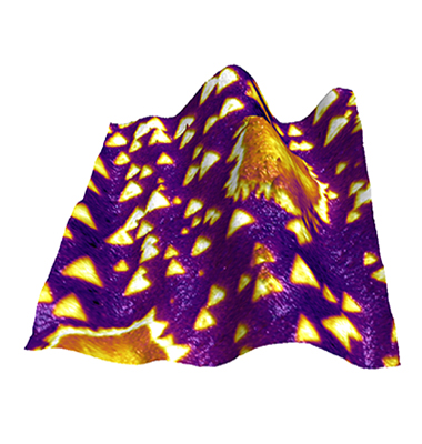
Figure caption: Kelvin Probe Force Microscopy surface potential overlaid on topography for flakes of boron nitride (small triangles) and graphene (large irregular features) grown on a copper foil substrate.

About Oxford Instruments Asylum Research

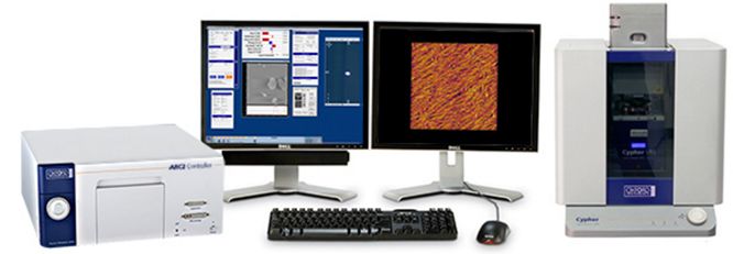
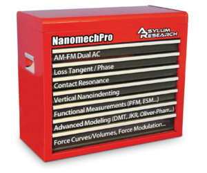
Oxford Instruments Asylum Research is the technology leader in atomic force microscopy for both materials and bioscience research. Asylum Research AFMs are widely used by both academic and industrial researchers for characterizing samples from diverse fields spanning material science, polymers, thin films, energy research, and biophysics. In addition to routine imaging of sample topography and roughness, Asylum Research AFMs also offer unmatched resolution and quantitative measurement capability for nanoelectrical, nanomechanical and electromechanical characterization. Recent advances have made these measurements far simpler and more automated for increased consistency and productivity.  Its Cypher™ and MFP-3D™ AFM product lines span a wide range of performance and budgets.  Asylum Research also offers its exclusive SurfRider™ AFM probes among a comprehensive selection of AFM probes, accessories, and consumables. Sales, applications and service offices are located in the United States, Germany, United Kingdom, Japan, France, India, China and Taiwan, with distributor offices in other global regions.

About Oxford Instruments plc

Oxford Instruments designs, supplies and supports high-technology tools and systems with a focus on research and industrial applications. Innovation has been the driving force behind Oxford Instruments’ growth and success for over 50 years, and its strategy is to effect the successful commercialisation of these ideas by bringing them to market in a timely and customer-focused fashion.

The first technology business to be spun out from Oxford University, Oxford Instruments objective is to be the leading provider of new generation tools and systems for the research and industrial sectors with a focus on nanotechnology. Its key market sectors include nano-fabrication and nano-materials. The company’s strategy is to expand the business into the life sciences arena, where nanotechnology and biotechnology intersect.

This involves the combination of core technologies in areas such as low temperature, high magnetic field and ultra high vacuum environments; Nuclear Magnetic Resonance; x-ray, electron, laser and optical based metrology; atomic force microscopy; optical imaging; advanced growth, deposition and etching.

Oxford Instruments aims to pursue responsible development and deeper understanding of our world through science and technology. Its products, expertise, and ideas address global issues such as energy, environment, security and health.

The NanomechPro ™ Toolkit:

Accurate Tools for Measuring Nanoscale Mechanical Properties for Diverse Materials

Understanding nanoscale mechanical properties is of fundamental importance for evaluating the behavior and performance of a wide NanomechProDSHR-1
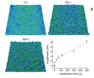
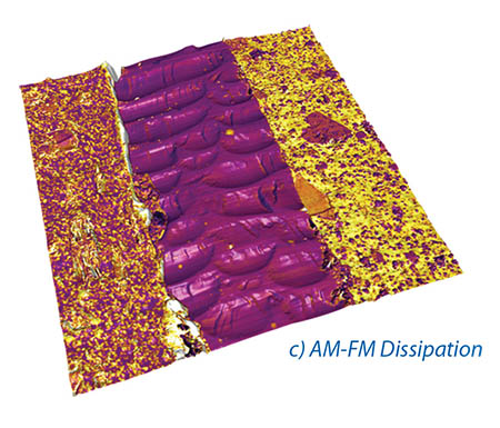
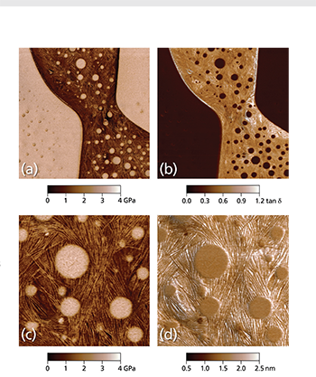
variety of industrially, biologically and structurally important materials. An Atomic Force Microscope (AFM) tip interacting with a sample experiences forces originating from many different sources – elasticity, viscosity, adhesion, van der Waals – to name a few. Hence, it has become increasingly clear that reliable and accurate materials properties measurements require looking at your sample in more than one way. Single techniques are simply insufficient for accurately and rigorously revealing sample properties and can often yield misleading and even inaccurate results and conclusions.

The NanomechPro™ toolkit (Figure 1) for Asylum’s Cypher™ and MFP-3D™ AFMs provides a suite of tools to meet the requirements of the nanomechanics researcher and is both impressively powerful and rapidly expanding. The various tools are complementary – each technique probes and records different responses of your samples – and often can be used  imultaneously (e.g. Figures 2a – d). Additionally, with the Cypher AFM, many of these new techniques can be combined with small, fast, low noise cantilevers, enabling measurements at noise levels and speeds previously impossible.

Combined Loss Tangent and AM-FM Imaging

Amplitude-modulated (AM) atomic force microscopy, also known as tapping mode or AC mode, is a proven, reliable and gentle imaging method with widespread applications. Previously, the contrast in tapping mode has been difficult to quantify. However, in this work we introduce two new techniques that allow unambiguous interpretation of material properties in tapping mode: AM-FM and Loss Tangent. Because these measurements are made simultaneously, there is a built-in check for self-consistency in the measurements. The new AM-FM imaging technique combines the features and benefits of normal tapping mode with the quantitative, high sensitivity of Frequency Modulation (FM) mode. Both Loss Tangent and AM-FM imaging can be performed simultaneously at high data acquisition rates. These techniques are exclusively available from Asylum Research, US patents 8,024,963, 7,937,991, 7,603,891, 7,921,466 and 7,958,563 with others pending.

download

Contact Resonance Viscoelastic Mapping Mode

Introduction

Asylum Research’s Contact Resonance Viscoelastic Mapping Mode option forthe MFP-3D™ and Cypher™ S atomic force microscopes (AFMs) enables high resolution, quantitative imaging of both elastic storage modulus and viscoelastic loss modulus. It is just one of the many anomechanical tools in Asylum’s NanomechPro™ Toolkit. The contact resonance technique is particularly well suited for characterizing moderate to high modulus materials in the range of about 1GPa to 200GPa. Thanks to recent advances by Asylum and our collaborators, Contact Resonance Viscoelastic Mapping Mode is now faster, more quantitative, and easier to use than earlier implementations.

How it works

The contact resonance principle

The contact resonance technique, first developed in the 1990s by the Yamanaka and Arnold groups,1,2 is based on the principle that the resonance of an AFM cantilever changes when it is in contact with a sample. As shown in Figure 1, the cantilever and sample in contact can be thought of as one spring coupled in series to a second spring and dashpot in parallel. Here, the first spring represents the elastic response of the cantilever and the second spring and dashpot represent the viscoelastic response of the sample. Therefore, as the stiffness of the sample contact changes, the frequency of the contact resonance changes (higher stiffness = higher frequency). Changes in the viscous response of the sample are reflected in the Quality factor (Q) of the contact resonance (more viscous = lower Q). Standard contact mechanics models can be used to then convert these stiffness and dissipation measurements to elastic modulus and loss modulus.

Contact resonance imaging

The contact resonance technique is based on contact mode imaging. This means that the AFM cantilever scans along the sample surface at a constant force (the setpoint), measured by the cantilever deflection. As the tip encounters higher (or lower) features, the tip-sample force begins to increase (or decrease). A feedback loop continuously adjusts the height up (or down) to keep the force at a constant value (the setpoint). This motion is recorded as the sample topography.

While the tip scans the sample in contact mode, the contact resonance is continuously changing with the sample mechanical properties. In order to measure the contact resonance, a very low amplitude vertical modulation is introduced by driving either the cantilever or the sample. The drive is at a relatively high frequency, so this modulation does not affect the contact mode feedback loop, but the modulation nevertheless couples to the cantilever deflection and can be measured using a lock-in amplifier.

download

New Scanning Probe Techniques for Analyzing

Organic Photovoltaic Materials and Devices

Rajiv Giridharagopal, Guozheng Shao, Chris Groves, and David S. Ginger Department of Chemistry, University of Washington, Seattle, WA 98195, USA

Abstract

Organic solar cells hold promise as an economical means of harvesting solar energy due to their ease of production and processing. However, the efficiency of such organic photovoltaic (OPV) devices is currently below that required for widespread adoption. The efficiency of an OPV is inextricably linked to its nanoscale morphology. High-resolution metrology can play a key role in the discovery and optimization of new organic semiconductors in the lab, as well as assist the transition of OPVs from the lab to mass production. We review the instrumental issues associated with the application of scanning probe microscopy techniques such as photoconductive atomic force microscopy and time-resolved electrostatic force microscopy that have been shown to be useful in the study of nanostructured organic solar cells. These techniques offer unique insight into the underlying heterogeneity of OPV devices and provide a nanoscale basis for understanding how morphology directly affects OPV operation. Finally, we discuss opportunities for further improvements in scanning probe microscopy to contribute to OPV development. All measurements and imaging discussed in this application note were performed with an Asylum Research MFP-3D-BIO™ Atomic Force Microscope.

Introduction

OPV materials are an emerging alternative technology for converting sunlight into electricity. OPVs are potentially very inexpensive to process, highly scalable in terms of manufacturing, and compatible with mechanically flexible substrates. In an OPV device, semiconducting polymers or small organic molecules are used to accomplish the functions of collecting solar photons, converting the photons to electrical charges, and transporting the charges to an external circuit as a useable current.1-3

At present, the most intensely-studied and highest-performing OPV systems are those that employ bulk heterojunction (or BHJ) blends as the active layer, with NREL-certified power conversion efficiencies improving seemingly monthly, and currently standing at 6.77%.4 In a bulk heterojunction blend, the donor and acceptor material are typically mixed in solution, and the mixture is then coated on the substrate to form the active layer. The donor/acceptor pair can consist of two different conjugated polymers, but it is often a conjugated polymer (donor) and a soluble fullerene derivative (acceptor).

download

AM-FM Viscoelastic Mapping Mode

Information on mechanical properties is important in many applications. AM-FM Viscoelastic Mapping Mode lets you quickly and gently image viscoelastic properties including storage modulus and loss tangent with nanoscale spatial resolution. Its very wide operating range, from less than 1 MPa to hundreds of GPa, makes it a highly versatile technique. AM-FM Mode is available on all MFP-3D™ and Cypher™ family AFMs and is one of many options in Asylum’s NanomechPro™ Toolkit for nanomechanical measurements.

Capabilities and Benefits

Asylum’s exclusive AM-FM Viscoelastic Mapping Mode1 is a flexible, convenient tool for nanomechanical characterization. With a range of applicability that spans a remarkable six orders of magnitude in storage modulus (from less than 1 MPa to hundreds of GPa), it is a general-purpose technique for anything from biomaterials and polymers to metals and ceramics. AM-FM Mode provides elastic information including storage modulus, Young’s modulus, and contact stiffness and viscoelastic information including viscoelastic loss tangent and loss modulus. AM-FM Mode gets results by operating at two cantilever resonances simultaneously. As the name indicates, the first resonance is used for tapping mode imaging, also known as amplitude modulation (AM), while a higher resonance mode is operated in frequency modulation (FM). At resonance, the cantilever frequency and phase respond sensitively to changes in sample properties. Small frequency and phase shifts can be measured with very high precision and accuracy, reducing uncertainty and increasing sensitivity. You can use raw output signals to quickly visualize relative contrast and identify sample components; or you can use the observed amplitude, phase, and frequency data to make quantitative estimates of mechanical properties based on built-in or your own models.

Because AM-FM Mode works like tapping mode in the repulsive regime, it is familiar and straightforward to use. It also has the other advantages of tapping mode including fast scanning, high spatial resolution, and gentle forces. On high speed, low-noise systems such as Asylum’s Cypher S and ES AFMs, modulus mapping in AM-FM Mode can routinely operate at line scan rates as fast as 20 Hz (equivalent tip velocity 300 μm/s) and forces as low as 50 pN.2 Low forces mean less sample deformation, typically only a few nanometers, which both minimizes damage and maximizes spatial resolution. Because the FM amplitude is just a tiny fraction of the AM amplitude and is at a different frequency, topographic imaging operates the same as in standard tapping mode. This makes AM-FM Mode very stable and reliable to operate.

download

Force Scanning with the MFP-3D™ AFMs: Two Capabilities In One

Atomic force microscopy (AFM) is able to reveal many properties about a material. Most commonly, it is used to obtain topographical information, but it can also probe mechanical stiffness, electrical conductance, resistivity, and magnetism. Researchers have used it to study interactions between enzymes and their substrates1, structural changes in injured or diseased tissue2, macromolecular interactions between lipids3 and analysis of nucleic acid organization and structure4, to name a few applications. AFM performs analyses on a micro and nanoscale, allowing it to quantify phenomena as miniscule as van der Waals forces, electrostatic interactions, and molecular bonds5. AFM is also able to produce high-resolution, detailed images of sample surfaces, displaying micro and nanoscale properties of materials as flat as cleaved mica or as non-uniform as a cell. An interesting aspect to AFM is its ability to measure multiple micro- and nanoscale properties in a single test on samples that are unfixed, unstained, and alive. Of particular use in many fields is the imultaneous measurement of topographical features and mechanical properties.

Traditional light microscopy is able to reveal a wealth of information about a sample, especially a biological one. Light microscopy can tell investigators the shape of a cell, localization of subcellular structures within the cell, and even organization of cellular infrastructure, among many other parameters. But a limitation with these optical data is that we are unable to measure, in a directly quantifiable way, the mechanical properties of that cell; these properties give investigators important information about the cell’s cytoskeletal organization and phenotype. The cell’s stiffness, quantified by measuring the elastic modulus of the cell, is different at various points across its surface; cells tend to be softer over the cytoplasm and stiffer over cytoskeletal structures. Generally speaking, AFM is able to assess both mechanical and topographical properties of any material, including cells, simultaneously in a single assay.


download